2.5D Topographies – 2 Cutting-Edge Solutions!
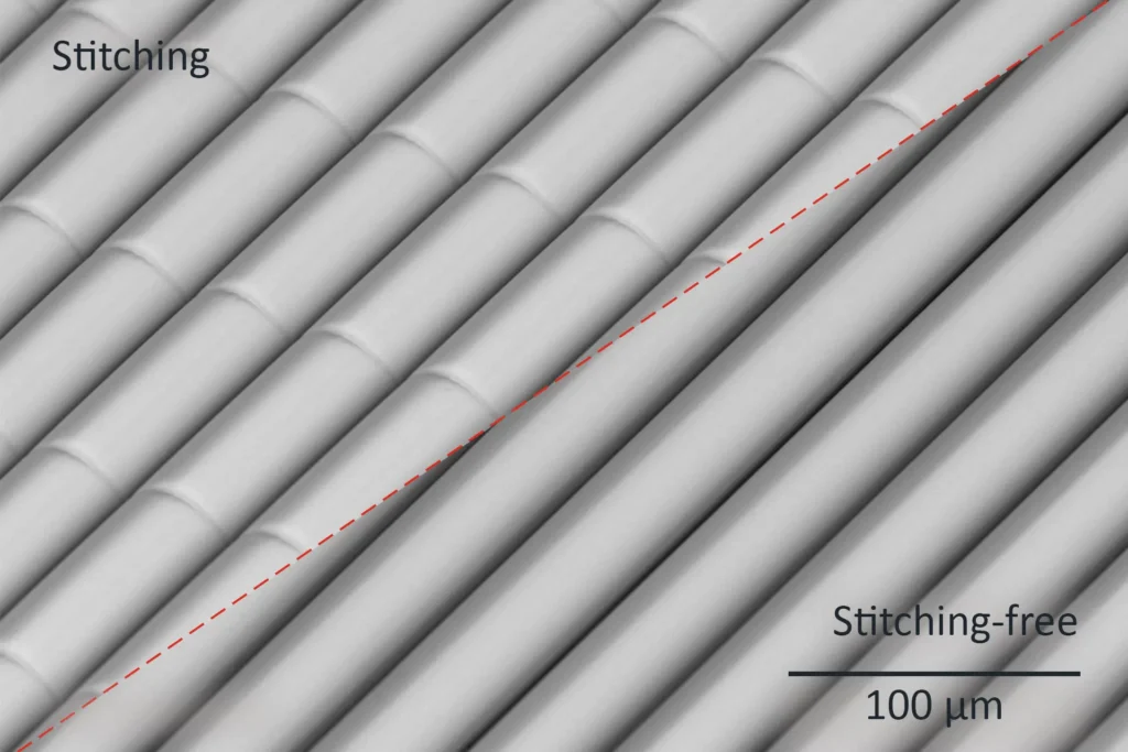
Advancing Excellence in Microfabrication: Fabrication of 2.5D Topographies with Maskless Grayscale Lithography or Two-Photon Polymerization (TPP) What looks like ocean waves or river pebbles is

Advancing Excellence in Microfabrication: Fabrication of 2.5D Topographies with Maskless Grayscale Lithography or Two-Photon Polymerization (TPP) What looks like ocean waves or river pebbles is

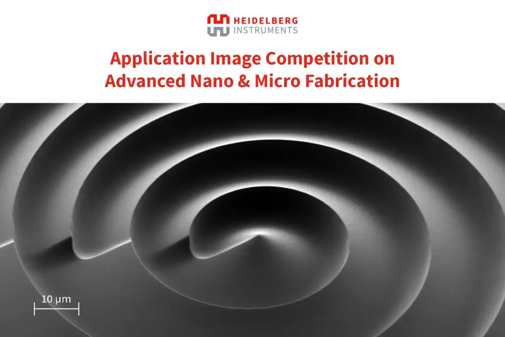
All users of Heidelberg Instruments and Multiphoton Optics products are invited to participate in our new “Application Image Competition on Advanced Nano & Micro Fabrication”.

We rely heavily on electronics for virtually everything we do. But actually, it does not necessarily need to be electrons that do all the job.

Scanning Tunnelling Microscopy (STM) relies on quantum tunnelling for imaging and manipulation of objects on atomic scale. It is one of the most precise techniques

Quantum computers are one of the most exciting developments of today’s physics. There are a lot of open questions in this field: on which technical

Research in many fields of modern physics requires micro- or nanoscale devices. Nanofabrication has achieved a truly amazing level of sophistication: physicists routinely deal with

We celebrate the National Nanotechnology Day (USA) on October 9th, which pays homage to the nanometer scale: 1 nm equals 1 x 10⁻⁹ m (one

The oldest light in the Universe is called Cosmic Microwave Background (CMB), or relic radiation. It began travelling through space when the universe became transparent

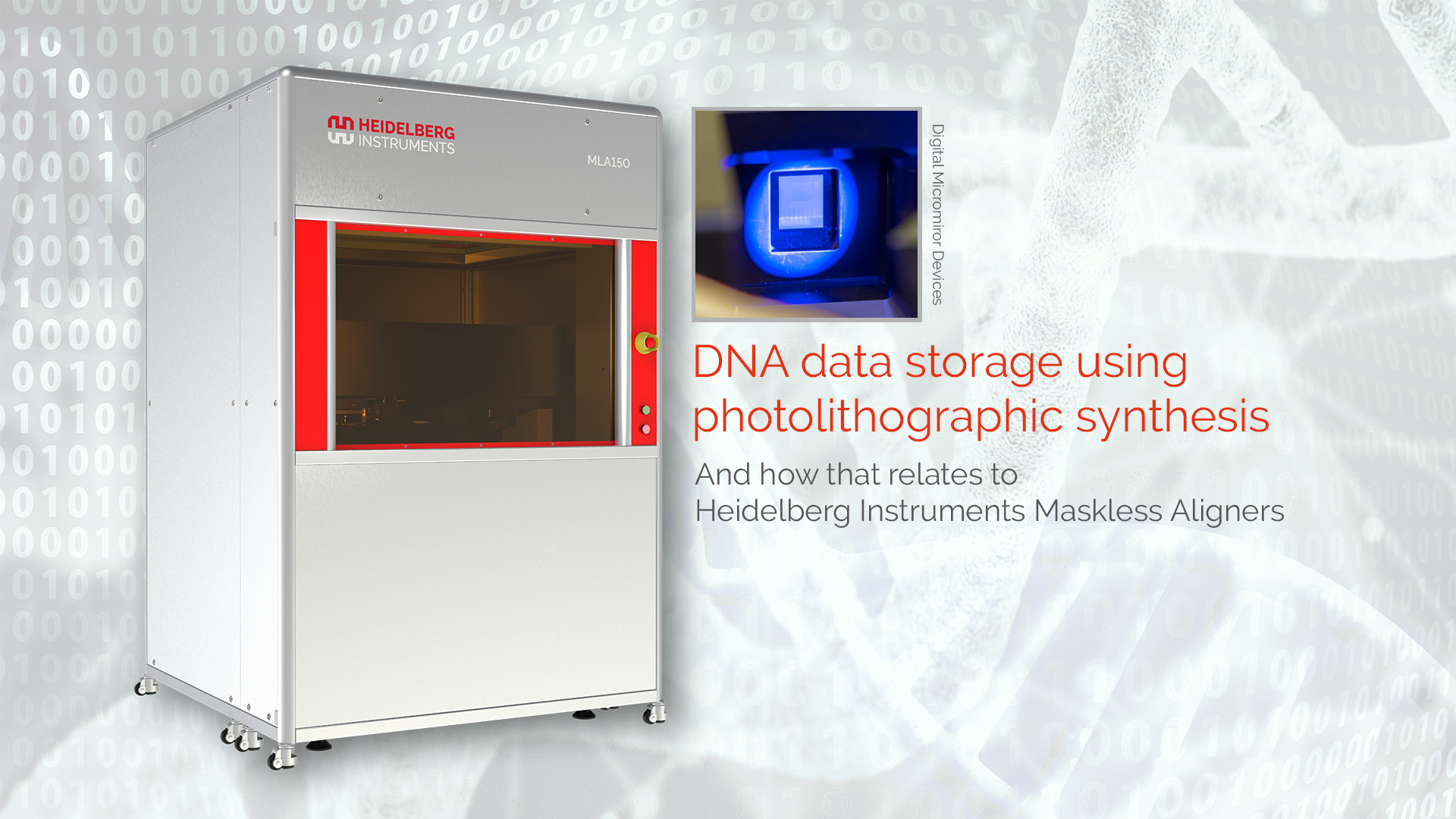
Lately, a Nature article inspired us to take a look at our MLA Maskless Aligner series. The authors described a low-cost approach to DNA data
The DWL 66+ is now more powerful than ever, featuring two game-changing enhancements that redefine what’s possible with optical lithography.

Direct Laser Writing accelerates the fabrication of custom infrared metasurfaces—enabling fast, flexible, and cost-effective beam shaping, holography, and more, without complex lithography.

Physicists have crafted the “world’s smallest violin” as a stunning demonstration of their new NanoFrazor nanolithography capabilities.

Read Heidelberg Instruments’ recap of the OPTICA Global Advanced Manufacturing Alliance Meeting 2025. Thanks to all for advancing photonics innovation!

Discover how researchers fabricated an ultra-thin flat lens (MDL) with the DWL 66+, offering a lightweight, cost-effective solution for true-color astrophotography and space-based imaging.

Explore the challenges and solutions in achieving deep grayscale lithography (>100 µm) for advanced microfabrication. Learn about resist limitations, mask requirements, and the advantages of direct laser writing.

Discover how the VPG+ 1400 FPD revolutionizes flat panel display fabrication with high-speed, sub-micron resolution photomask writing. Designed for OLED, micro-LED, and quantum dot displays, it delivers unmatched precision, scalability, and throughput for next-generation FPD manufacturing.

Sustainable microfabrication is the future. Explore how Heidelberg Instruments’ advanced lithography solutions reduce waste, energy use, and chemical consumption.

The close of 2024 marked a unique chapter in Heidelberg Instruments’ history. For the first time in our 40 years,

On December 3 and 4, Heidelberg Instruments hosted the project meeting of the EU-funded FABulous initiative at its Würzburg location.
Follow us on social media to benefit
from a range of useful resources.