High & Ultra-High Resolution
300 nm with Optical and 15 nm with Thermal Scanning Probe Lithography
-
Description
-
Resolution can be much more than just the smallest feature size possible. Depending on the application, the deciding factor for high resolution can be feature density, restrictions on geometry, line-edge roughness, or CD uniformity.
In ultra-high resolution-lithography, for resolutions of below 100nm in size, the actual process for resist choice and etching, as well as the metrology functionality, become critical factors.
The specifications that we provide for our lithography systems are conservative and are easily achievable during the site acceptance, meaning that the exposure results from our systems could be better than what is advertised (as shown in a few examples).
We strive to push technology to the physical limits of resolution. Our optical systems can reach dimensions down to 300 nm, while our NanoFrazor thermal scanning probe lithography systems can achieve 15 nm isolated feature sizes using the ultra-sharp heated tips.
Related images


Suitable Systems

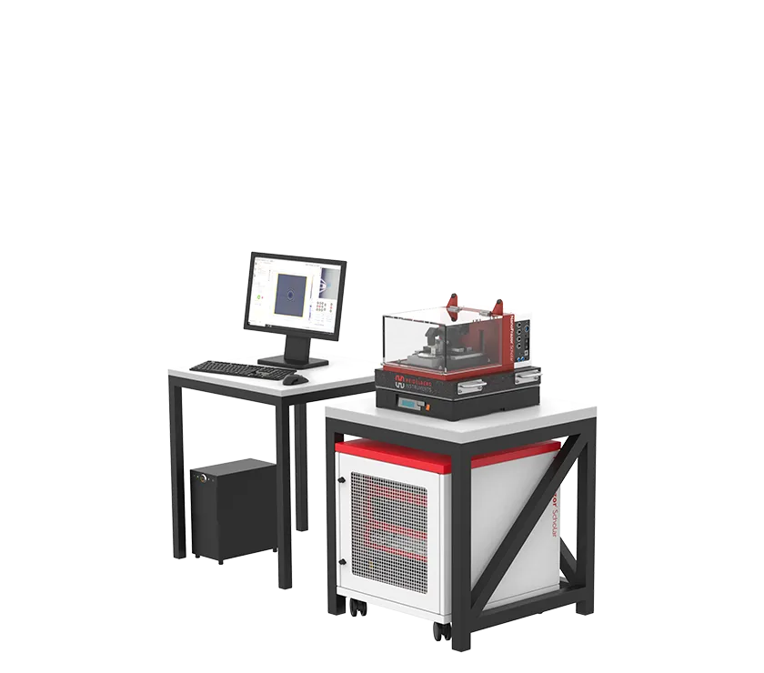
NanoFrazor Scholar
- Thermal Scanning Probe Lithography System
Table-top thermal scanning probe lithography system with in-situ AFM imaging. Compact and compatible with glovebox.

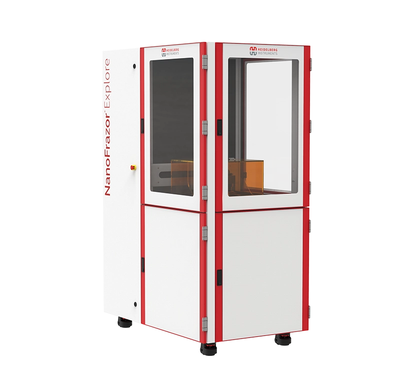
NanoFrazor Explore
- Thermal Scanning Probe Lithography System
Thermal scanning probe lithography tool with direct laser sublimation and grayscale modules. Excellent alternative to e-beam lithography tools.

