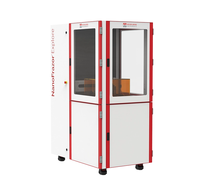
NanoFrazor Explore
- Thermal Scanning Probe Lithography System
Thermal scanning probe lithography tool with direct laser sublimation and grayscale modules. Excellent alternative to e-beam lithography tools.
Description
Thermal Scanning Probe Lithography (t-SPL) is a patterning method in which a thermally sensitive resist is sublimated using an ultra-sharp heated tip. This method allows for complex, high-resolution nanostructures to be both written and visually inspected on the same tool.
This approach forms the very core of the NanoFrazor operating principle. After patterning, standard pattern transfer methods such as lift-off or etching can then be applied to the patterned substrates. This technology first appeared at IBM Research Zürich in the framework of the Millipede memory project, which then evolved into a complete nanofabrication method. The technology is now commercially available from Heidelberg Instruments in the form of our NanoFrazor Scholar and NanoFrazor Explore systems.
The NanoFrazor technology represents an alternative to conventional nanofabrication methods. It allows both high-resolution patterning as well as imaging with a scan speed of 1 mm/s. This method avoids many problems some of the other nanolithography techniques exhibit – no wet development, no proximity effect corrections, and no vacuum is required. The compatibility with any standard pattern transfer process and substrate material opens up a wide range of applications.


Thermal scanning probe lithography tool with direct laser sublimation and grayscale modules. Excellent alternative to e-beam lithography tools.

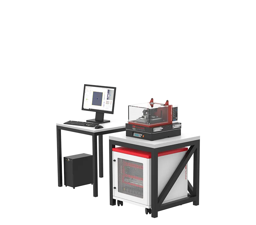
Table-top thermal scanning probe lithography system with in-situ AFM imaging. Compact and compatible with glovebox.
We are always at your disposal.
Please send us your request.
To view the form, please enable Marketing cookies.
Subscribe to our newsletter
to receive the newest information.
To view the form, please enable Marketing cookies.