
MPO 100 successfully installed at Kyoto University
Exciting news! At Kyoto University Nanotechnology Hub one MPO 100 3D microprinting system and one MLA 150 maskless lithography system
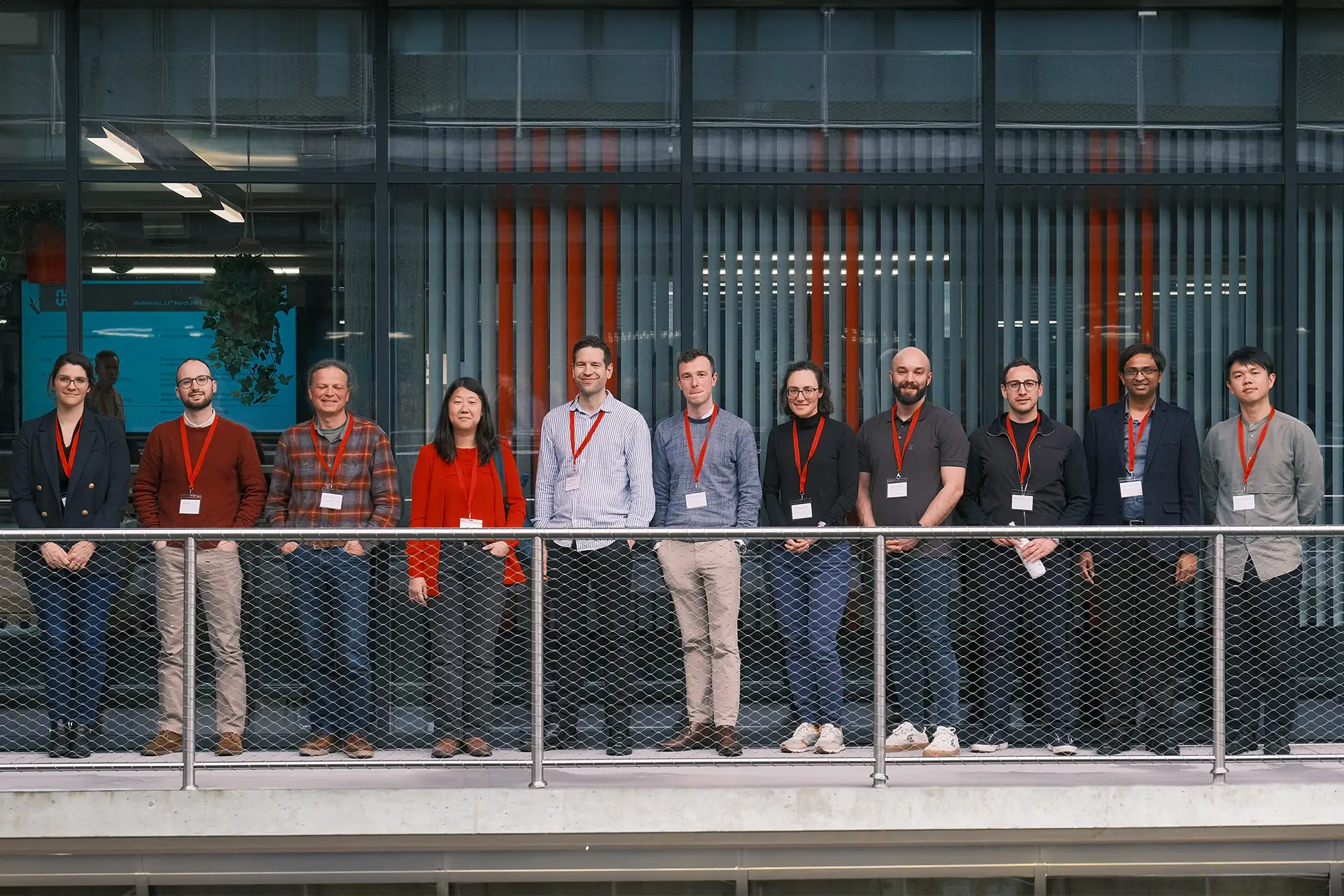
Thermal Probe Workshop 2024 – Thank You for a Successful Event
A look back on the 8th Thermal Probe Workshop We were delighted to host a community of nanotechnology experts, fabrication
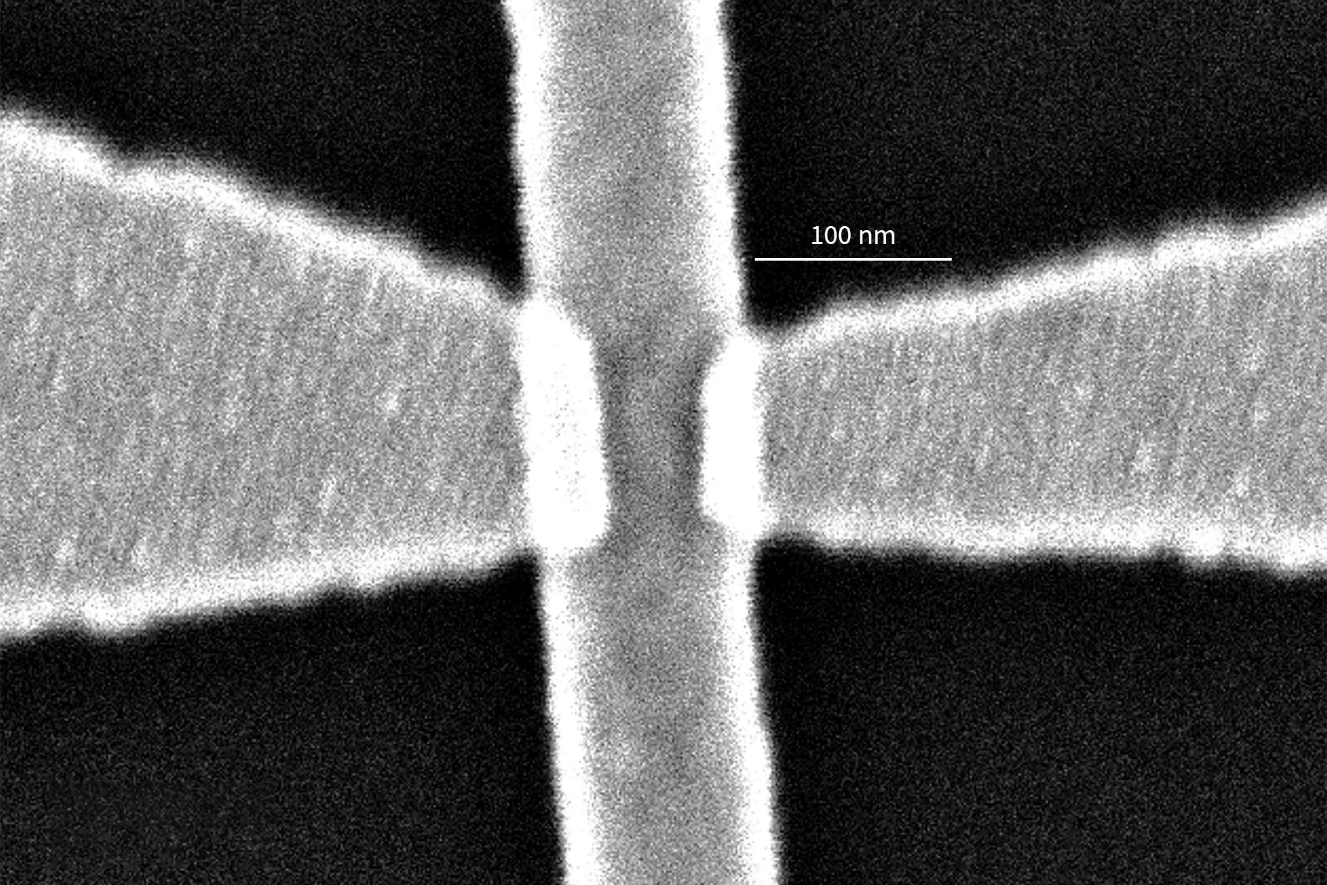
Combining one- and multiphoton direct laser writing
Achieve high throughput and resolution. Despite its unique capacity for three-dimensional fabrication with minimal feature sizes below 100 nm, achieving
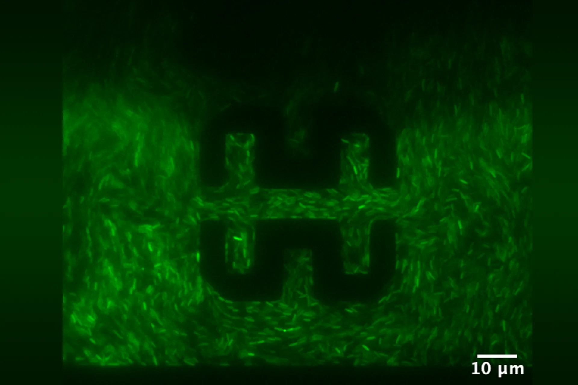
Effective Pattern Transfer after NanoFrazor Lithography
Discover our two Application Notes covering this topic: “Bilayer Lift-Off for NanoFrazor Lithography”“Ultra-High Resolution Pattern Transfer on NanoFrazor Lithography” In
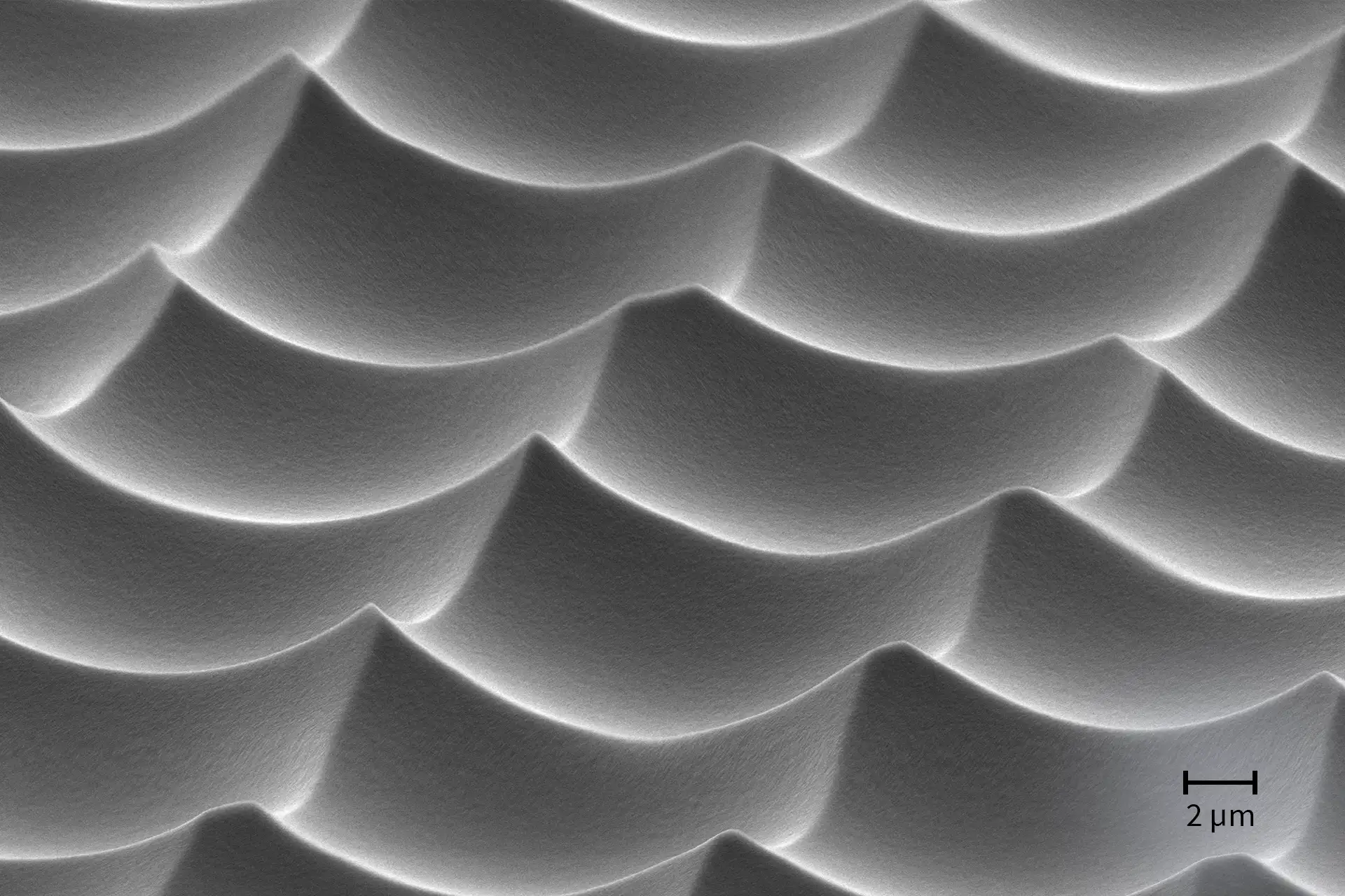
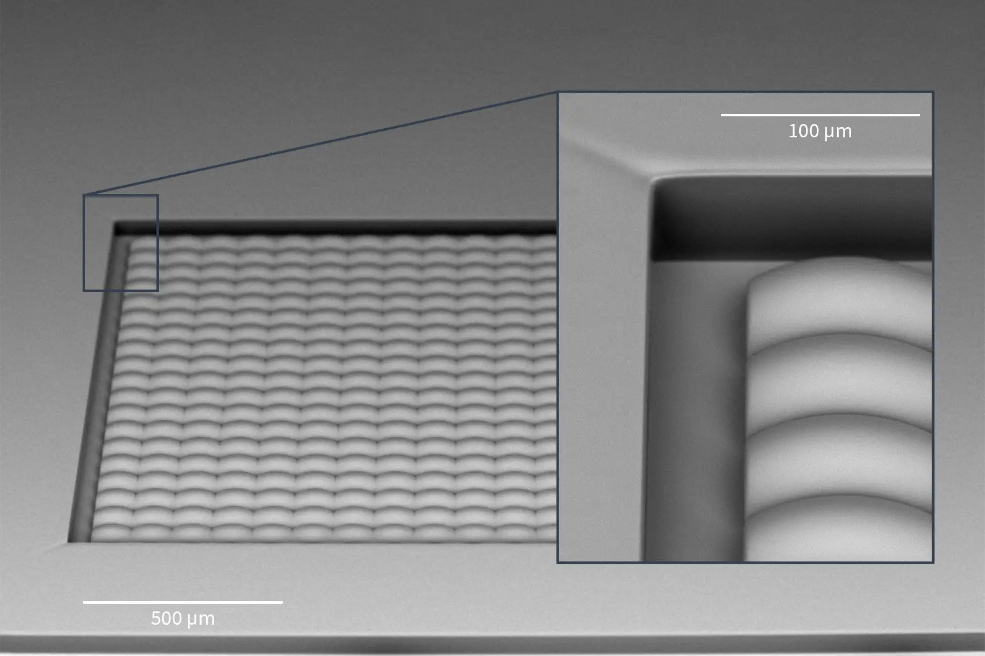
2.5D Topographies – 2 Cutting-Edge Solutions!
Advancing Excellence in Microfabrication: Fabrication of 2.5D Topographies with Maskless Grayscale Lithography or Two-Photon Polymerization (TPP) What looks like ocean
New Year’s greetings from CEO Konrad Roessler
2024 will mark Heidelberg Instruments‘ 40th anniversary. With gratitude we look back, with joy we look forward to what’s ahead.

Seasons’ Greeting from Heidelberg Instruments
Season’s Greetings from Heidelberg Instruments! In the spirit of joy and gratitude, we extend our warmest wishes to our valued
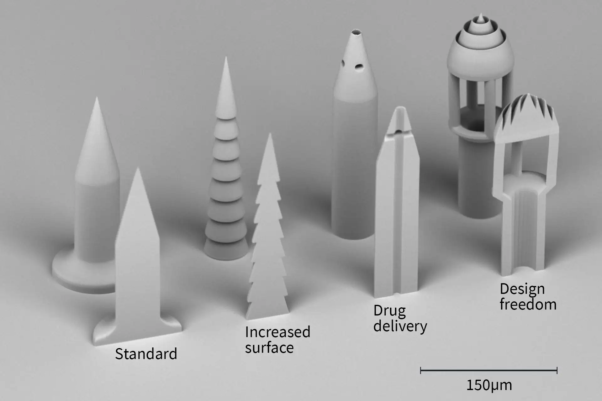
3D Printed Drug Delivery Devices
Microneedles as alternative to conventional drug administration Commonly used methods of drug delivery are associated with certain drawbacks: As an
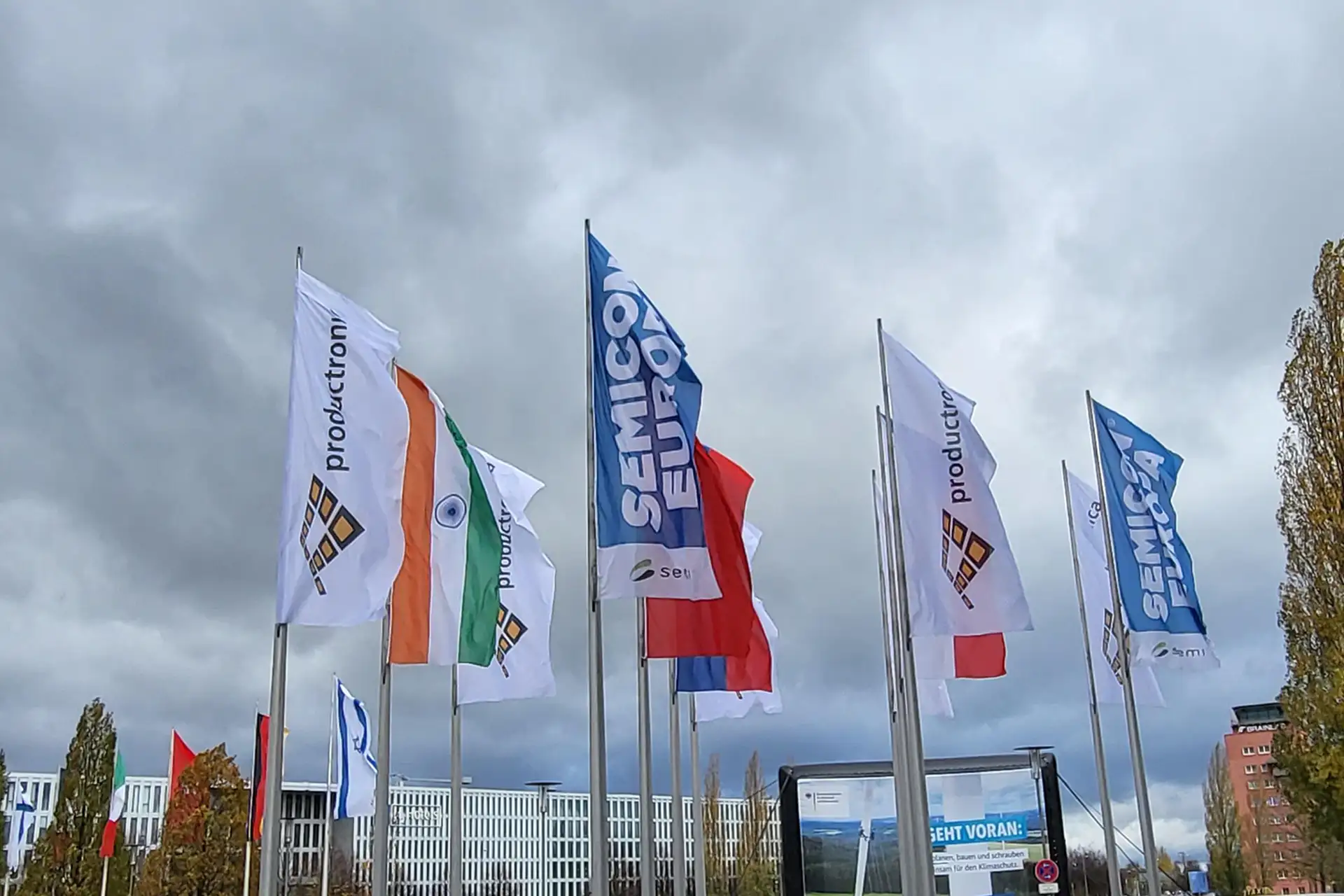
SEMICON Europa 2023 at a glance
The Heidelberg Instruments booth at SEMICON EUROPA 2023 in Munich from November 14th -17th attracted a wide range of visitors
Winners of Application Image Competition receive certificates
The EIPBN conference, which stands for the International Conference on Electron, Ion, and Photon Beam Technology and Nanofabrication, and is
MPO 100 successfully installed at Kyoto University
Exciting news! At Kyoto University Nanotechnology Hub one MPO 100 3D microprinting system and one MLA 150 maskless lithography system
Thermal Probe Workshop 2024 – Thank You for a Successful Event
A look back on the 8th Thermal Probe Workshop We were delighted to host a community of nanotechnology experts, fabrication
Combining one- and multiphoton direct laser writing
Achieve high throughput and resolution. Despite its unique capacity for three-dimensional fabrication with minimal feature sizes below 100 nm, achieving
Effective Pattern Transfer after NanoFrazor Lithography
Discover our two Application Notes covering this topic: “Bilayer Lift-Off for NanoFrazor Lithography”“Ultra-High Resolution Pattern Transfer on NanoFrazor Lithography” In
2.5D Topographies – 2 Cutting-Edge Solutions!
Advancing Excellence in Microfabrication: Fabrication of 2.5D Topographies with Maskless Grayscale Lithography or Two-Photon Polymerization (TPP) What looks like ocean
New Year’s greetings from CEO Konrad Roessler
2024 will mark Heidelberg Instruments‘ 40th anniversary. With gratitude we look back, with joy we look forward to what’s ahead.
Seasons’ Greeting from Heidelberg Instruments
Season’s Greetings from Heidelberg Instruments! In the spirit of joy and gratitude, we extend our warmest wishes to our valued
3D Printed Drug Delivery Devices
Microneedles as alternative to conventional drug administration Commonly used methods of drug delivery are associated with certain drawbacks: As an
SEMICON Europa 2023 at a glance
The Heidelberg Instruments booth at SEMICON EUROPA 2023 in Munich from November 14th -17th attracted a wide range of visitors
Winners of Application Image Competition receive certificates
The EIPBN conference, which stands for the International Conference on Electron, Ion, and Photon Beam Technology and Nanofabrication, and is