Designed to produce mature semiconductor photomasks
-
Product Description
-
The ULTRA is a qualified laser mask writer specifically for mature semiconductor photomasks. Semiconductor photomasks are used to fabricate electronic devices including microcontrollers, power management, LED, Internet of Things (IoT) and MEMS.
The ULTRA is an economical mask writer solution with all the features and functionality required for high throughput, precision and structure uniformity, and extremely accurate alignment. The standard configuration includes features like full automatic mask handling, Zerodur® stage, low distortion optics and high-precision position control.
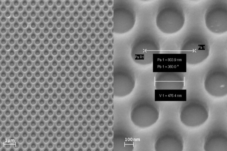
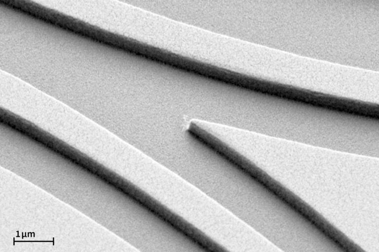
ULTRA systems can produce structure sizes down to 500 nm at write speeds up 580 mm2 per minute, while featuring excellent critical dimension uniformity, image quality, overlay and registration. As a compact system, it fits easily into the existing mask shop infrastructure.The ULTRA is a qualified laser mask writer specifically for mature semiconductor photomasks. Semiconductor photomasks are used to fabricate electronic devices including microcontrollers, power management, LED, Internet of Things (IoT) and MEMS.
The ULTRA is an economical mask writer solution with all the features and functionality required for high throughput, precision and structure uniformity, and extremely accurate alignment. The standard configuration includes features like full automatic mask handling, Zerodur® stage, low distortion optics and high-precision position control.
ULTRA systems can produce structure sizes down to 500 nm at write speeds up 580 mm2 per minute, while featuring excellent critical dimension uniformity, image quality, overlay and registration. As a compact system, it fits easily into the existing mask shop infrastructure. -
Product Highlights
-
High Exposure Quality
Custom High NA write lens and low distortion UV-opticsHigh Precision
Full air-bearing stage; zero thermal expansion ZERODUR® chuck; high resolution differential interferometer; stage corrections and tool matching functionsHigh Throughput
Fast SLM based exposure engine; fast mode; 6“ write time below 45 minutes -
Available Modules
-
The ULTRA is a qualified laser mask writer specifically for mature semiconductor photomasks. Semiconductor photomasks are used to fabricate electronic devices including microcontrollers, power management, LED, Internet of Things (IoT) and MEMS.
The ULTRA is an economical mask writer solution with all the features and functionality required for high throughput, precision and structure uniformity, and extremely accurate alignment. The standard configuration includes features like full automatic mask handling, Zerodur® stage, low distortion optics and high-precision position control.
ULTRA systems can produce structure sizes down to 500 nm at write speeds up 580 mm2 per minute, while featuring excellent critical dimension uniformity, image quality, overlay and registration. As a compact system, it fits easily into the existing mask shop infrastructure.
High Exposure Quality
High Precision
High Throughput
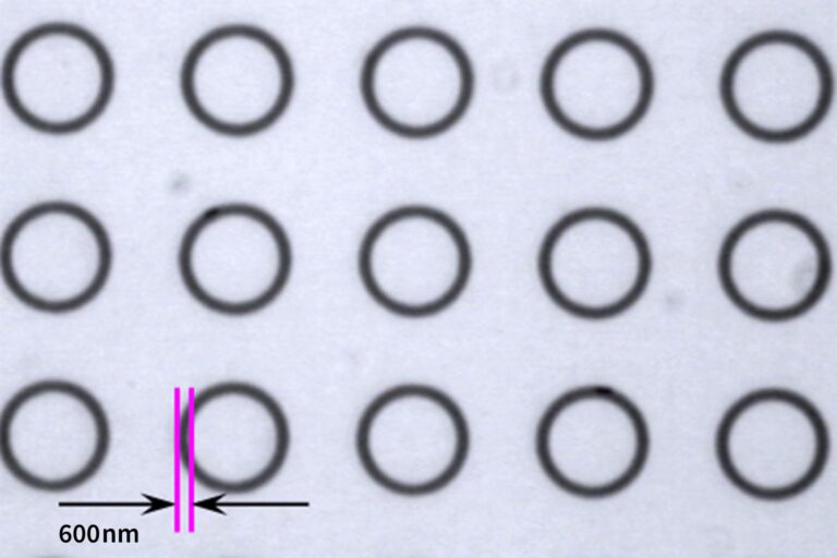
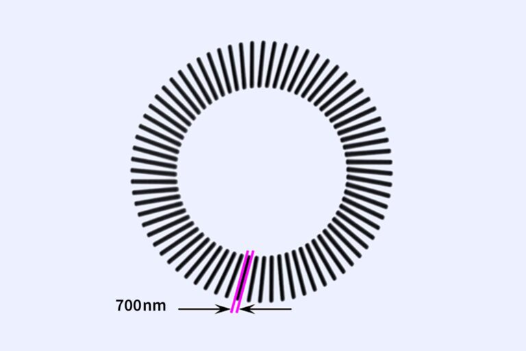
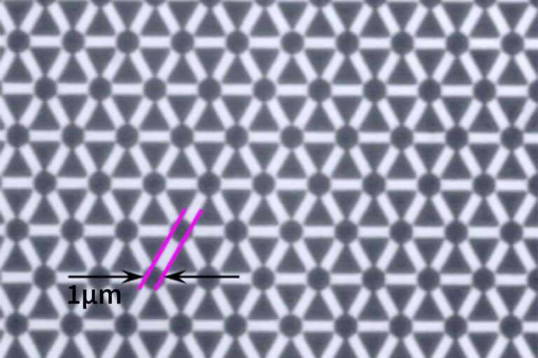
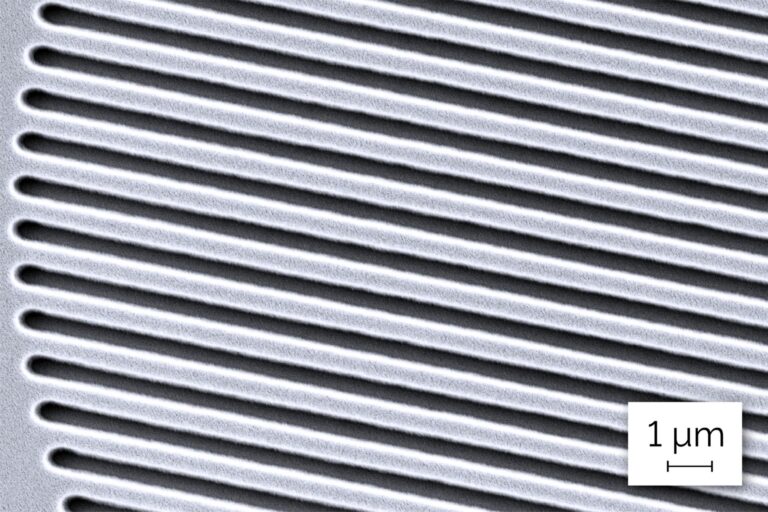
Customer applications
Technical Data
| QX mode | FX mode | |
|---|---|---|
| Writing performance | ||
| Address grid [nm] | 4 | 10 |
| Line edge roughness [3σ, nm] | 20 | 40 |
| Position accuracy [3σ, nm] | 40 | 100 |
| Overlay [3σ, nm] | 30 | 60 |
| Stitching [3σ, nm] | 20 | 60 |
| 2nd layer alignment [max error / nm] | 100 | 100 |
| CD uniformity [3σ, nm] | 30 | 60 |
| Minimum feature size [nm] | 500 | 700 |
| Write speed [mm² / min] | 325 | 580 |
| Write time for 6″ x 6″ [min] | 75 | 45 |
| Operation | |
|---|---|
| User interface (software) | SEMI-compliant GUI |
| Maximum write area | 228 x 228 mm² (others on request) |
| Substrate size | 4", 5", 6", 7", and 9" masks (larger and other substrates on request) |
| System features | |
| Optics | 0.9 NA objective lens Low-distortion UV optics Automatic calibration routines |
| Laser | High power diode pumped solid state laser with 355nm wavelength |
| Focus system | Real-time optical autofocus |
| Alignment | Camera system Distortion compensation Global and Field-by-field alignment Edge detector |
| Data path | Real-time compression Scalable hardware concept Input formats: All standard formats, e.g. GDSII and Jobdeck |
| Spatial Light Modulator | Frequency 350 kHz Data rate 2.4 GB/s |
| Automation | Full automatic mask handling with two carrier stations up to 9“; optional SECS/GEM protocols |
| System dimensions | System / Electronic rack |
| Width [mm] | 2995 / 800 |
| Depth [mm] | 1652 / 650 |
| Height [mm] | 2102 / 1800 |
| Weight [kg] | 3400 / 180 |
| Installation requirements | |
| Electrical | 400 VAC ± 5%, 50/60 Hz, 16A, 3 phases |
| Compressed air | 7 - 10 bar (without oil or other residue) |
Please note
Specifications depend on individual process conditions and may vary according to equipment configuration. Write speed depends on pixel size and write mode. Design and specifications are subject to change without prior notice.