Lithography can modify or deteriorate sample properties, e.g., by exposure to high-energy charged particles like electrons or ions. This can lead to the unwanted creation of covalent bonds with the organic resist, trapped charges, or lattice defects. The resulting contaminations or defects can significantly deteriorate device performance when using chip designs with insulating layers or devices comprising sensitive materials like 2D materials or nanowires.
The heated tip of the standard NanoFrazor lithography process only heats the top resist layer. Sensitive materials below the resist stack are not heated perceptibly and remain completely unharmed during patterning of the top resist layer.
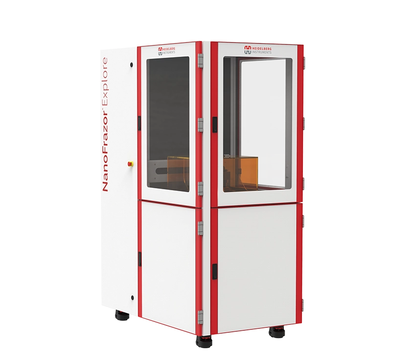
The NanoFrazor can also be incorporated inside a glovebox, which facilitates nanolithography on samples that deteriorate in air.