Advancements in microelectronics continuously rely on shrinking electronic devices and incorporating novel materials in active regions to achieve ever-higher speeds and new functionalities in device structures. This exploration of device architectures and use of new materials necessitates a rapid prototyping approach, enabling efficient testing and implementation of design changes.
Maskless lithography tools like the MLA, DWL and VPG+ series of Heidelberg Instruments, have emerged as a transformative technology in microelectronics lithography, offering numerous advantages compared to traditional photolithography. Their high resolution and maskless operation enable precise patterning of intricate microscale features, driving the limits of miniaturization. By eliminating physical masks, production costs are reduced, and rapid prototyping becomes feasible, accelerating development cycles. The technology’s flexibility allows for on-the-fly customization, tailoring each device on the wafer according to specific requirements.
The NanoFrazor facilitates nanoelectronics by combining Thermal Scanning Probe Lithography (t-SPL) with Direct Laser Sublimation. This thermal nanolithography technique enables the creation of nanostructures in the most critical regions of devices with the highest resolutions. The incorporation of laser direct sublimation of the same thermal resists allows for efficient writing of electrical traces and contacts. As a result, the NanoFrazor has become an ideal choice for nanoelectronic device fabrication, particularly in applications such as quantum electronics and molecular sensing.
Critical insulating layers not impacted by charged particles
Accurate overlay
using alignment marks or none. The functional structured layer can be used as reference (NanoFrazor and Draw Mode)
Ultra-high resolution (15 nm)
without the need for proximity effect corrections (NanoFrazor)
High resolution
Minimum feature size 300 nm (DWL 66+)
Advancements in microelectronics continuously rely on shrinking electronic devices and incorporating novel materials in active regions to achieve ever-higher speeds and new functionalities in device structures. This exploration of device architectures and use of new materials necessitates a rapid prototyping approach, enabling efficient testing and implementation of design changes.
Maskless lithography tools like the MLA, DWL and VPG+ series of Heidelberg Instruments, have emerged as a transformative technology in microelectronics lithography, offering numerous advantages compared to traditional photolithography. Their high resolution and maskless operation enable precise patterning of intricate microscale features, driving the limits of miniaturization. By eliminating physical masks, production costs are reduced, and rapid prototyping becomes feasible, accelerating development cycles. The technology’s flexibility allows for on-the-fly customization, tailoring each device on the wafer according to specific requirements.
The NanoFrazor facilitates nanoelectronics by combining Thermal Scanning Probe Lithography (t-SPL) with Direct Laser Sublimation. This thermal nanolithography technique enables the creation of nanostructures in the most critical regions of devices with the highest resolutions. The incorporation of laser direct sublimation of the same thermal resists allows for efficient writing of electrical traces and contacts. As a result, the NanoFrazor has become an ideal choice for nanoelectronic device fabrication, particularly in applications such as quantum electronics and molecular sensing.
Dense patterns with high resolution features and low line edge roughness
Precise overlay of several layers
Compatibility with existing pattern transfer processes
Fast turnaround time with high flexibility
Fast prototyping
No mask required
No charge accumulation
Critical insulating layers not impacted by charged particles
Accurate overlay
using alignment marks or none. The functional structured layer can be used as reference (NanoFrazor and Draw Mode)
Ultra-high resolution (15 nm)
without the need for proximity effect corrections (NanoFrazor)
High resolution
Minimum feature size 300 nm (DWL 66+)
Application images
A very accurate overlay between a nanowire and contacts can be achieved by imaging the sample topography with the sharp tip beforehand.
(NanoFrazor, Courtesy of Heidelberg Instruments Nano)
Sharp vertical Ag electrodes made with the NanoFrazor tip.
(Courtesy of Prof. Leuthold group, ETH Zurich, Publication in 2019)
Single-electron transistors patterned with the mix & match NanoFrazor system using thermal probe for the sub-25 features and integrated laser writing for the contact wires.
(Courtesy of Imperial college and IBM Research, Publication in 2018)
Sensor devices and digital circuits made in several layers of materials using a DWL 66fs as part of research made in the direction of flexible electronics.
(Courtesy if IPN – Mexico)
Personalized contacts layer on prefabricated CMOS master, contact on poly-Si (ligh colour) and contacts on p-/n-well (dark colour)
(Courtesy of IMS Chips)
suitable Systems
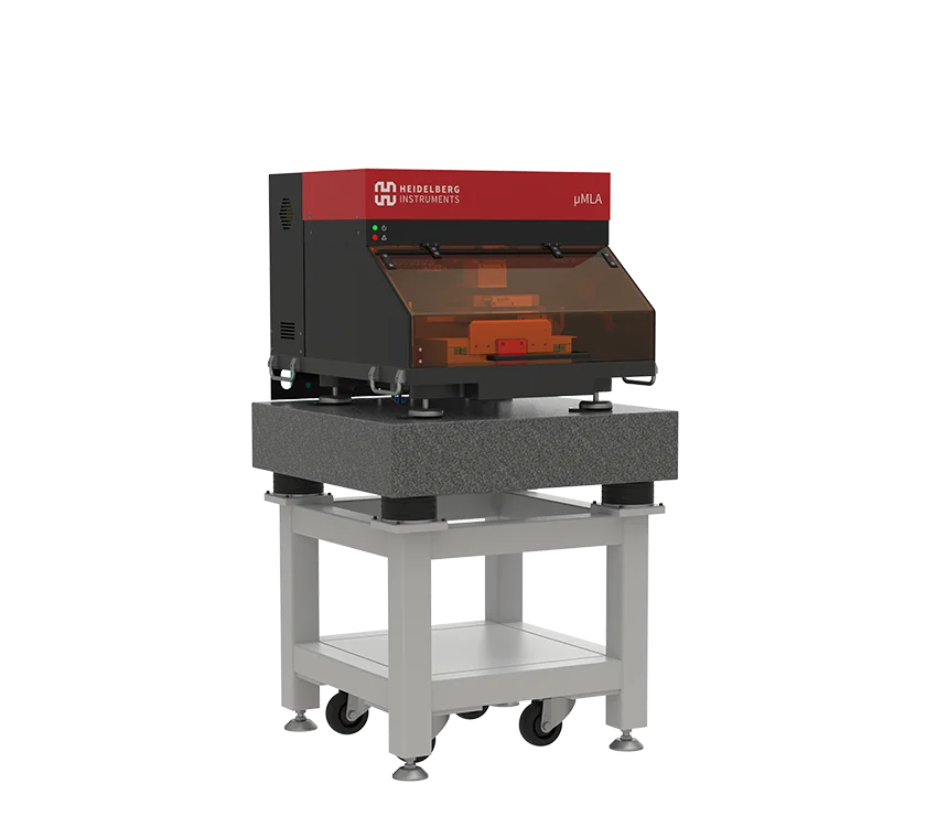
µMLA
Maskless Aligner
Configurable and compact tabletop maskless aligner with raster scan and vector exposure modules.
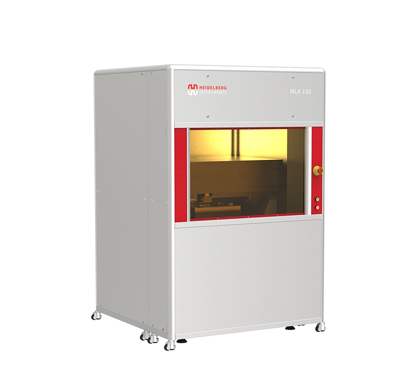
MLA 150
Maskless Aligner
The fastest maskless tool for rapid prototyping, the alternative to the mask aligners. Perfect for standard binary lithography.
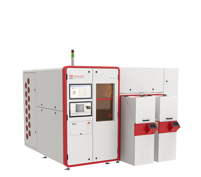
MLA 300
Maskless Aligner
Optimized for industrial production with highest throughput and seamless integration into industrial production lines.
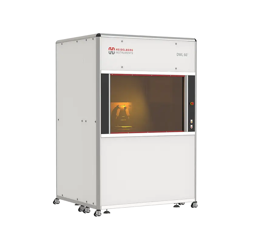
DWL 66+
Direct Write Laser Lithography System
Our most versatile system for research and prototyping with variable resolution and wide selection of options.
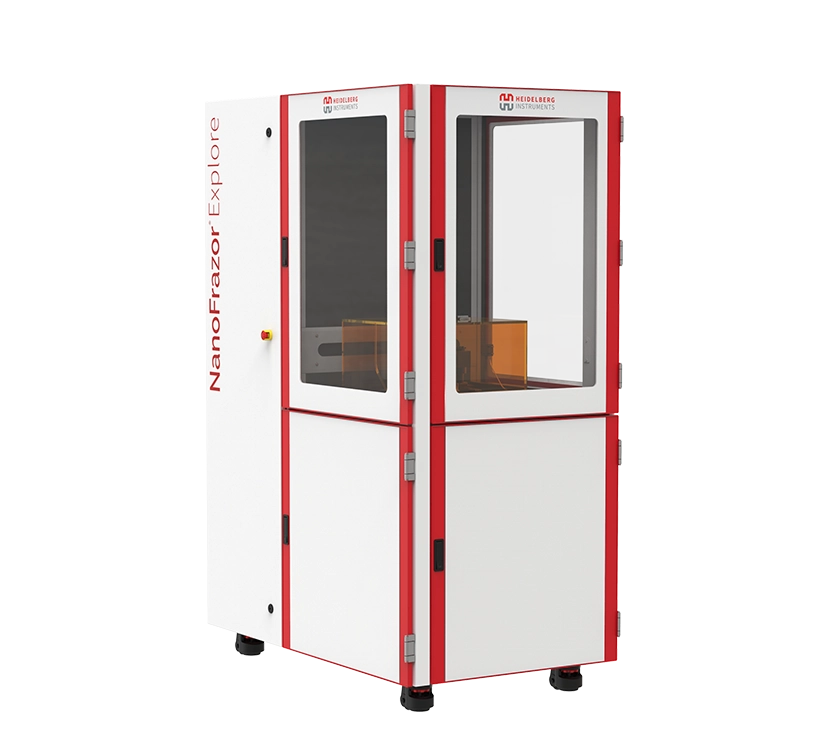
NanoFrazor Explore
Thermal Scanning Probe Lithography System
Thermal scanning probe lithography tool with direct laser sublimation and grayscale modules. Excellent alternative to e-beam lithography tools.