Successful 7th Edition of the Thermal Probe Workshop hosted by Heidelberg Instruments Nano
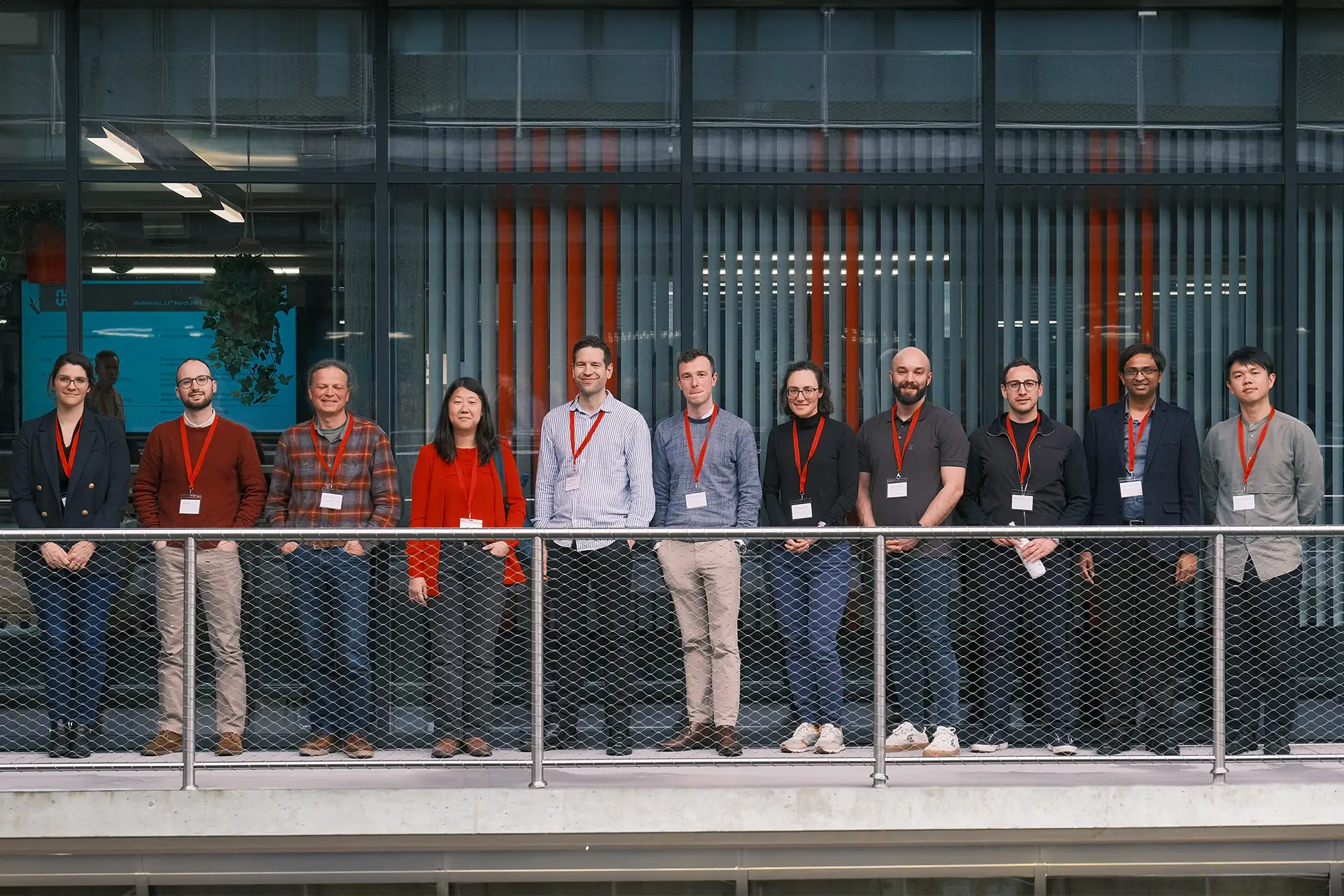
After a break of more than three years due to the pandemic, the international Thermal Scanning Probe Lithography community gathered at Heidelberg Instruments Nano in Zurich, Switzerland from March 15 – 16, 2023 to discuss innovative manufacturing methods and a wide range of applications employing heated tips. More than 80 participants from research groups all over the world discussed recent discoveries and exchanged experiences.
Following the opening remarks by Dr. Emine Cagin and Matthias Bürke from the Heidelberg Instruments Nano Board of Directors on the first day, the keynote speaker Prof. Juergen Brugger from École Polytechnique Fédérale de Lausanne began the first session on “Innovative Nanofabrication” by presenting a history of hot tip nanoengineering. Insightful sessions on “Pushing the Limits of t-SPL” and “Nanostructured Surfaces” followed soon after.
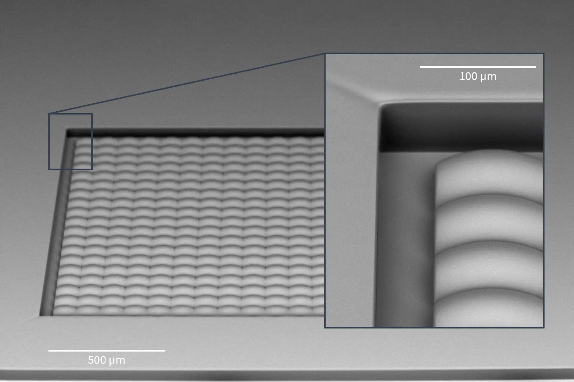
The day was rounded off with a poster session from participants and live demos of NanoFrazor’s 3D capabilities, where attendees could get their “nano-selfies” printed by the NanoFrazor.
Impressions from day 1


Insightful talks and discussions
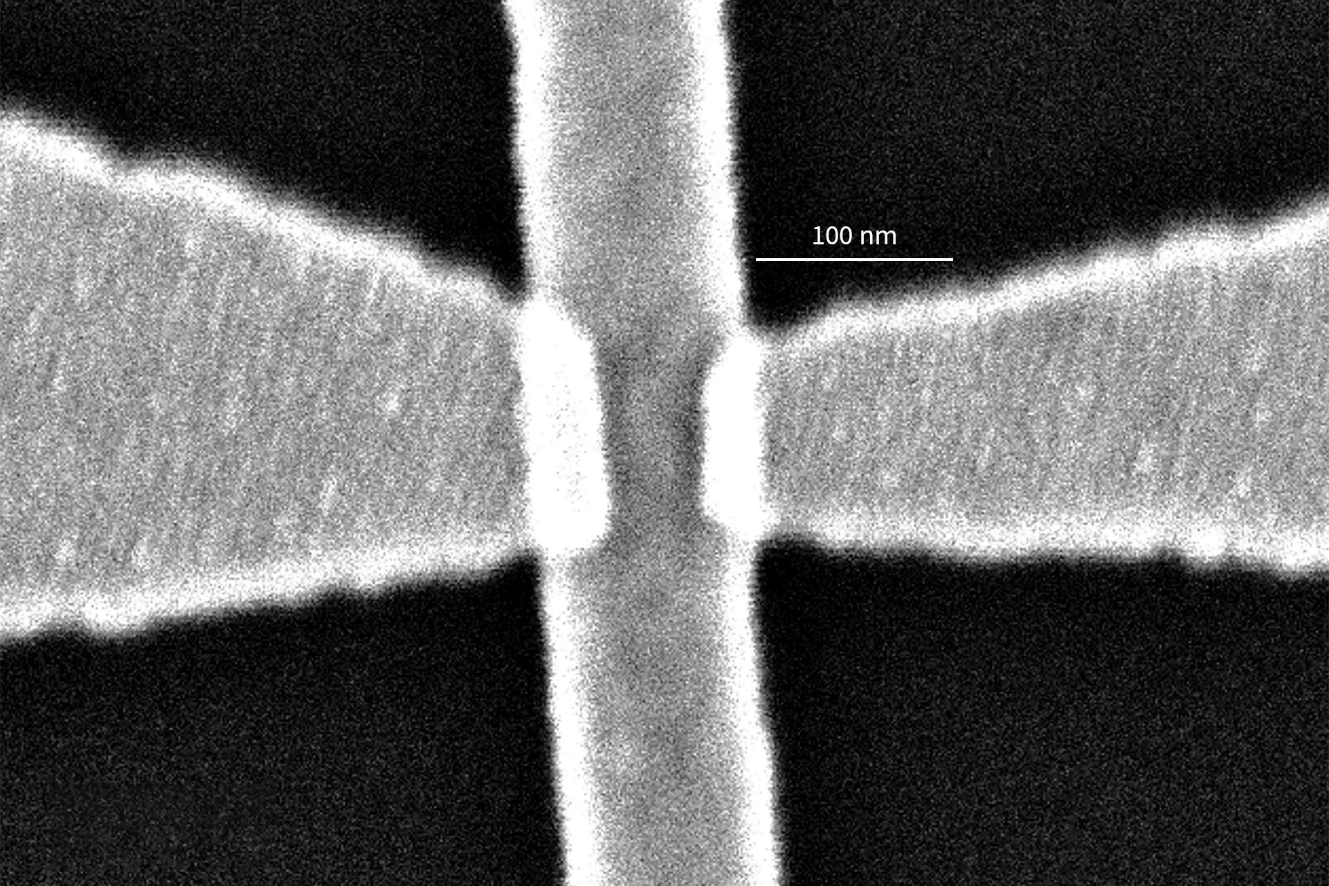
The second day kicked off with a session on Quantum Devices, where Dr. Armin Knoll from IBM Research Europe – Zurich shared his approach for reliable and automated batch fabrication of complex devices such as field effect transistors. The second session of the day dealt with the topic of 1D and 2D materials, with talks on 1D and 2D device fabrication and the thermal sculpting of nanocircuits. The workshop’s last session focused on advanced lithography materials.
Impressions from day 2


Overall, the Thermal Probe Workshop featured very interesting talks and discussions. The workshop ended with the announcement of the Best Poster award, which went to Dr. Chloe Bureau-Oxton from IBM Research Europe – Zurich for her poster on “An on-tip fin field-effect transistor as a scanning electrometer.”

We would like to take this opportunity to thank the speakers for their interesting presentations, the poster presenters for their works, and finally our Swiss colleagues for the perfect organization.
The workshop was a full success, and the feedback from the participants more than positive. The 8th Thermal Probe Workshop in 2024 is already set. More updates will follow soon!
Thermal Scanning Probe Lithography (t-SPL) is one of the three Heidelberg Instruments’ core technologies representing an alternative to conventional nanofabrication methods, and allowing both high-resolution patterning as well as imaging.
Always stay updated and follow Heidelberg Instruments on LinkedIn.
Heidelberg Instruments NanoFrazor systems
The technology behind the system is the result of more than 20 years of intensive research and development (R&D) that started at IBM Research Zürich and now takes place at Heidelberg Instruments Nano. The NanoFrazor hardware and software are constantly advancing to extend the capabilities and performance of the tool and the wide range of applications. Our dedicated team of experts continues to develop and optimize the pattern transfer processes for different applications. We compile this know-how in a growing library of best practices and protocols to support our customers.
Visit our product pages to learn more:
Talk to our experts
Heidelberg Instruments is attending exhibitions and conferences all over the world. Meet our experts at premier events like EIPBN or other events near you.