Heidelberg Instruments direct writers enable high precision, making them suitable for sensors with fine details and complex geometries (VPG & DWL series). They can work with a variety of materials, including polymers, metals, and ceramics. This flexibility is advantageous for creating sensors with diverse functional layers and optimizing the material properties for specific sensing applications.
Maskless lithography systems are valuable tools for rapid prototyping of sensor designs. Researchers and engineers can quickly iterate and test different sensor configurations without the need for time-consuming mask changes or complex lithography setups (VPG 300 DI, MLA series).
Two-Photon Polymerization allows for the fabrication of three-dimensional structures, which can be beneficial for sensors with complex architectures or those requiring specific spatial arrangements of sensing elements (MPO 100).
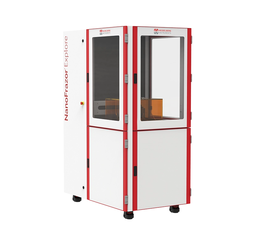
Thermal Scanning Probe Lithography with resolution capabilities as fine as 20 nm has the potential to elevate the sensitivity of the manufactured sensor. It opens up new possibilities for the development of sophisticated sensors and other nanoscale technologies.
between 355 nm and 405 nm (Direct writers), 522 nm for 3D through Two-Photon Polymerization (TPP) (MPO 100)
Heidelberg Instruments direct writers enable high precision, making them suitable for sensors with fine details and complex geometries (VPG & DWL series). They can work with a variety of materials, including polymers, metals, and ceramics. This flexibility is advantageous for creating sensors with diverse functional layers and optimizing the material properties for specific sensing applications.
Maskless lithography systems are valuable tools for rapid prototyping of sensor designs. Researchers and engineers can quickly iterate and test different sensor configurations without the need for time-consuming mask changes or complex lithography setups (VPG 300 DI, MLA series).
Two-Photon Polymerization allows for the fabrication of three-dimensional structures, which can be beneficial for sensors with complex architectures or those requiring specific spatial arrangements of sensing elements (MPO 100).
Thermal Scanning Probe Lithography with resolution capabilities as fine as 20 nm has the potential to elevate the sensitivity of the manufactured sensor. It opens up new possibilities for the development of sophisticated sensors and other nanoscale technologies.
Resolution
Flexibility
Precise overlay of several layers
Patterning of various materials
Accurate overlay
using alignment marks or none. The functional structured layer can be used as reference (NanoFrazor®, µMLA, MLA 150)
Ultra-high resolution (15 nm) without the need for proximity effect corrections
between 355 nm and 405 nm (Direct writers), 522 nm for 3D through Two-Photon Polymerization (TPP) (MPO 100)
Application images
mr-DWL exposed with a DWL 66+ with 405nm wavelength; comb of lines with varying lengths (linewidth & gap 50 µm)
Fabrication of sensor and digital circuits as part of the research made in the direction of flexible electronics. Multi-Layer thin-film transistor made of six different materials. (Courtesy of Instituto Politécnico Nacional (IPN), Mexico)
Pattern exposed in AZ positive resist (~3µm) aligned to a pattern structured in a wafer. The structured wafer contains a stack of three metals.
Part of Bolometer, 500nm gap in 700nm AZ MIR 701 positive resist. Courtesy of Tian Yuan Global Corp.
Part of Bolometer, 750nm gap in 700nm AZ MIR 701 positive resist. Courtesy of Tian Yuan Global Corp.
SQUID (Superconducting QUantum Interference Device) made with up to 18 layers process (Lift-off, plating, etching). Critical alignment requirements through thick layers. Yield increased by a factor 3 compared to mask aligners. (Courtesy of Kirchhoff Institute for Physics, Heidelberg)
Overlay exposure of a 5x5 Matrix of image sensors in SiGe SPADs (Single Photon Avallanche Diode) (Courtesy of IMS Chips)
Line Detector in SiGe-SPADs (single photon avalanche diodes made of silicon-germanium) - SEM cross-section (Courtesy of IMS Chips)
Structured photoresist of the Metal conductor tracks for SiGe-SPADs (single photon avalanche diodes made of silicon-germanium) (Courtesy of IMS Chips)
Freeform optic printed on-device: a EEL (Edge Emitting Laser), used for Beam Shaping in Sensors. (Courtesy of nanoplus Nanosystems and Technologies GmbH)
An SEM image of a 20 nm gap in between two metal electrodes patterned by NanoFrazor and transferred via a 3-layer lift-off process
suitable Systems
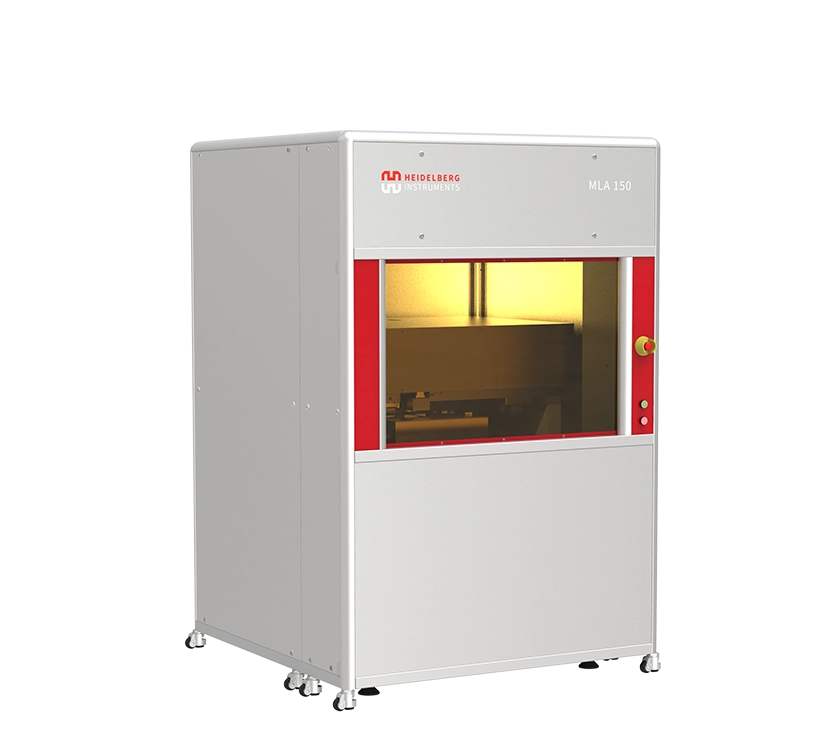
MLA 150
Maskless Aligner
The fastest maskless tool for rapid prototyping, the alternative to the mask aligners. Perfect for standard binary lithography.
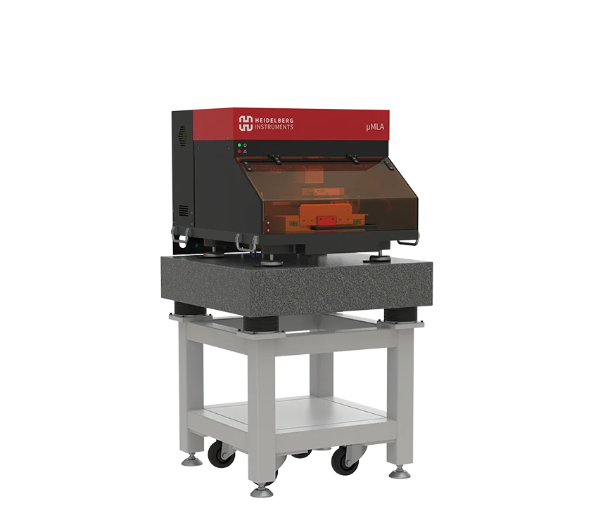
µMLA
Maskless Aligner
Configurable and compact tabletop maskless aligner with raster scan and vector exposure modules.
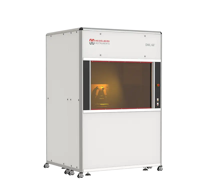
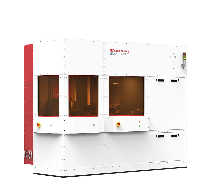
DWL 66+
Direct Write Laser Lithography System
Our most versatile system for research and prototyping with variable resolution and wide selection of options.
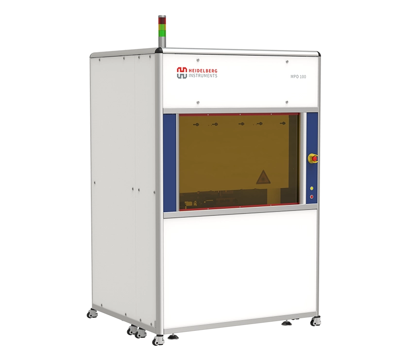
MPO 100
Two-Photon Polymerization Multi-User Tool
Multi-User Tool for 3D Lithography and 3D Microprinting of microstructures with applications in micro-optics, photonics, micro-mechanics and biomedical engineering.
NanoFrazor Explore
Thermal Scanning Probe Lithography System
Thermal scanning probe lithography tool with direct laser sublimation and grayscale modules. Excellent alternative to e-beam lithography tools.