Get a sneak peek into current material related research and further prospects.
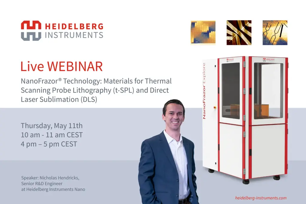
Our webinars on our NanoFrazor Technology cover a variety of topics around its operational capabilities and range of applications. Register for our webinar in May and gain valuable insights on our state-of-the-art Thermal Scanning Probe Lithography (t-SPL) and the important role of Polyphthalaldehyde (PPA), the main t-SPL resist. In our Webinar, Dr. Nicholas Hendricks will explain its capabilities and how PPA derivatives exceedingly advance t-SPL. Understand how resist is sublimated with the NanoFrazor Direct Laser Sublimation (DLS) modules and see for yourself how thin film optimization allows uniform DLS processing, over topography and heterogeneous surfaces. Alternative t-SPL resist within NanoFrazor tools will also be covered. At the end of the session there will be time for a Q&A.
Dr. Nicholas Hendricks studied chemistry focusing on Polymer at Wright University, specializing in polymer and materials for semiconductors and optical applications at University of Massachusetts Amherst. He obtained his Ph.D. in polymer science and engineering. His former employers incl. renowned institutions and companies such as Wright Patterson Air Force Base, Intel, British Petroleum and Federal Motors working in photolithography process development and more.
At Heidelberg Instruments, Nick holds a leading position in research and development on resist materials and transfer processing of patterns. His experience and knowledge contribute significantly to the advancements of the NanoFrazor technology.
European and American time zones
Thursday, 11.5.2023 | 10 AM CEST
Thursday, 11.5.2023 | 4 PM CEST | 9 AM CDT