Micro-lens arrays and complex Fresnel lenses are crucial components in compact camera optics due to the increasing demand for advanced and miniaturized optics in smartphones and tablets. These micro-lenses are used in a variety of applications such as wave-front sensors, fiber coupling, or homogenizing light sources. The production of these micro-lenses begins with grayscale lithography to generate a mold, which can then be replicated via LIGA to create a metal shim, used as a master tool for molding, imprinting, or hot embossing. Grayscale lithography is also used to fabricate micro-prisms, waveguides, blazed gratings, CGH (Computer Generated Holograms) and specialty security labels, among others. Direct Write Lithography enables the precise manufacturing of VLS (Variable Line Spacing) and standard gratings. The DWL series includes various high-performance Grayscale lithography systems, such as DWL 66+ for R&D and the DWL 2000 GS/ DWL 4000 GS for high-end requirements.
The MPO 100 utilizes Two-Photon Polymerization (TPP) to generate refractive and diffractive micro-optical elements with arbitrary shapes, providing unlimited design freedom compared to conventional techniques. This allows for the creation of miniaturized devices with multiple functions. With the MPO 100, individual micro-lenses or arrays can be fabricated directly on photonic chips, substrates, or optical fibers for endoscopic devices for in- and outcoupling purposes. Additionally, replication masters can be manufactured, providing mass production capabilities of sophisticated optical designs.
The NanoFrazor systems are powerful tools that can be used for a variety of micro-and nano-optic applications. Their high resolution associated with their grayscale lithography capabilities make them ideal for fabricating nano-optical structures such as diffraction gratings, optical Fourier surfaces, phase plates and more intricate finely tuned optical components.
Allowing smooth surfaces of large micro-optical elements in thick photoresist
Substrates from small pieces to G8 panel sizes
Our systems offer the possibility to choose the right stage size for your application
Shape optimization
Used to simplify the compensation of the nonlinear effects
High precision stage system for accurate pattern placement
Used to perfectly position micro-optic devices
Application specific write mode to optimize resolution and throughput
The choice of write modes enables to make the right compromise for your application (DWL series)
Micro-lens arrays and complex Fresnel lenses are crucial components in compact camera optics due to the increasing demand for advanced and miniaturized optics in smartphones and tablets. These micro-lenses are used in a variety of applications such as wave-front sensors, fiber coupling, or homogenizing light sources. The production of these micro-lenses begins with grayscale lithography to generate a mold, which can then be replicated via LIGA to create a metal shim, used as a master tool for molding, imprinting, or hot embossing. Grayscale lithography is also used to fabricate micro-prisms, waveguides, blazed gratings, CGH (Computer Generated Holograms) and specialty security labels, among others. Direct Write Lithography enables the precise manufacturing of VLS (Variable Line Spacing) and standard gratings. The DWL series includes various high-performance Grayscale lithography systems, such as DWL 66+ for R&D and the DWL 2000 GS/ DWL 4000 GS for high-end requirements.
The MPO 100 utilizes Two-Photon Polymerization (TPP) to generate refractive and diffractive micro-optical elements with arbitrary shapes, providing unlimited design freedom compared to conventional techniques. This allows for the creation of miniaturized devices with multiple functions. With the MPO 100, individual micro-lenses or arrays can be fabricated directly on photonic chips, substrates, or optical fibers for endoscopic devices for in- and outcoupling purposes. Additionally, replication masters can be manufactured, providing mass production capabilities of sophisticated optical designs.
The NanoFrazor systems are powerful tools that can be used for a variety of micro-and nano-optic applications. Their high resolution associated with their grayscale lithography capabilities make them ideal for fabricating nano-optical structures such as diffraction gratings, optical Fourier surfaces, phase plates and more intricate finely tuned optical components.
Very precise shape control
Excellent surface roughness
High throughput
No stitching artefacts
High resolution
Flexible substrate material and sizes for different applications
Diffraction gratings: Strict requirements for surface quality, groove position, and groove profile
Allowing smooth surfaces of large micro-optical elements in thick photoresist
Substrates from small pieces to G8 panel sizes
Our systems offer the possibility to choose the right stage size for your application
Shape optimization
Used to simplify the compensation of the nonlinear effects
High precision stage system for accurate pattern placement
Used to perfectly position micro-optic devices
Application specific write mode to optimize resolution and throughput
The choice of write modes enables to make the right compromise for your application (DWL series)
Application images
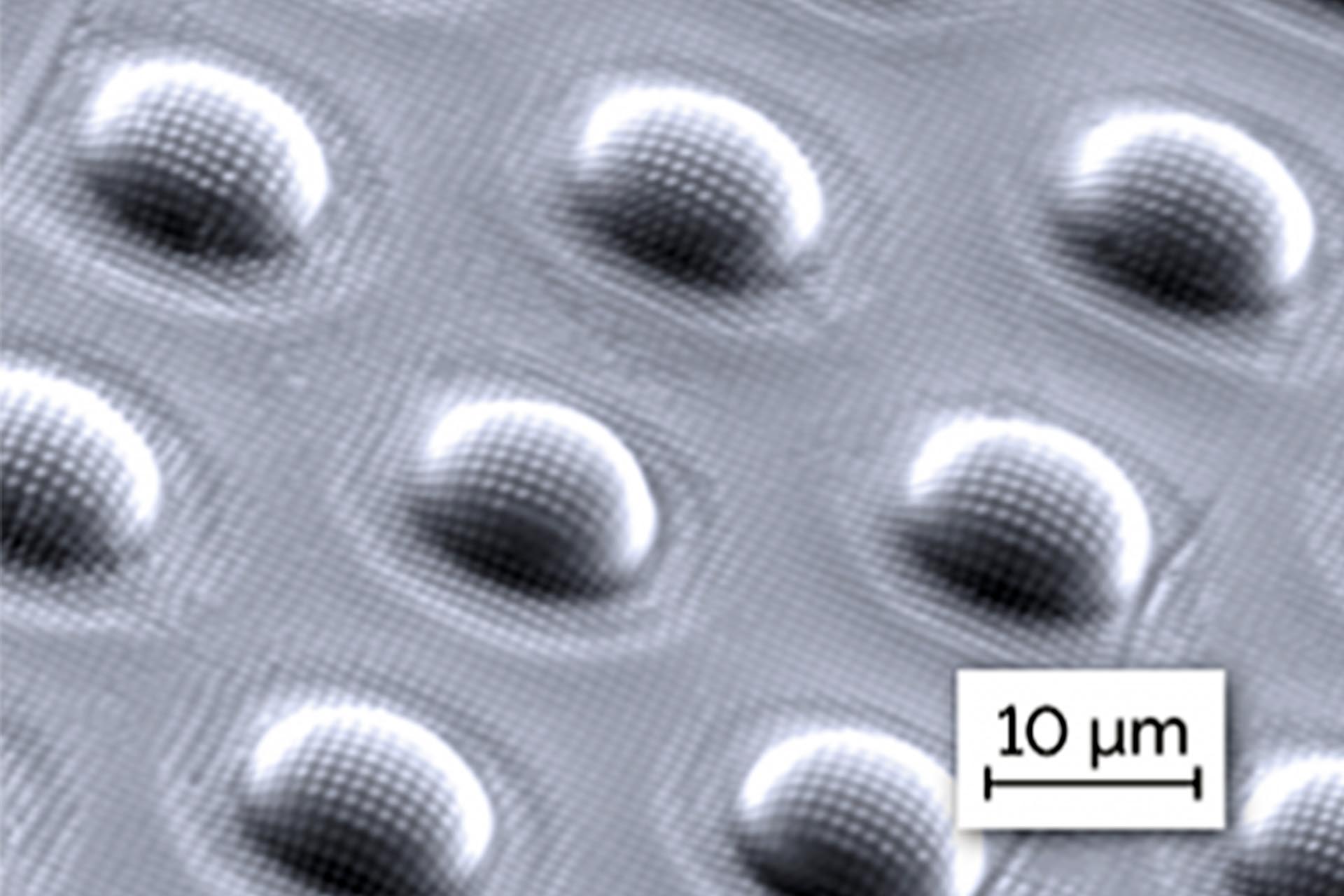
Irregular Microlens Array - Concave - Pseudo-square arrangement of lenslet. ~18µm (Average side) and ~6µm depth in AZ4562.
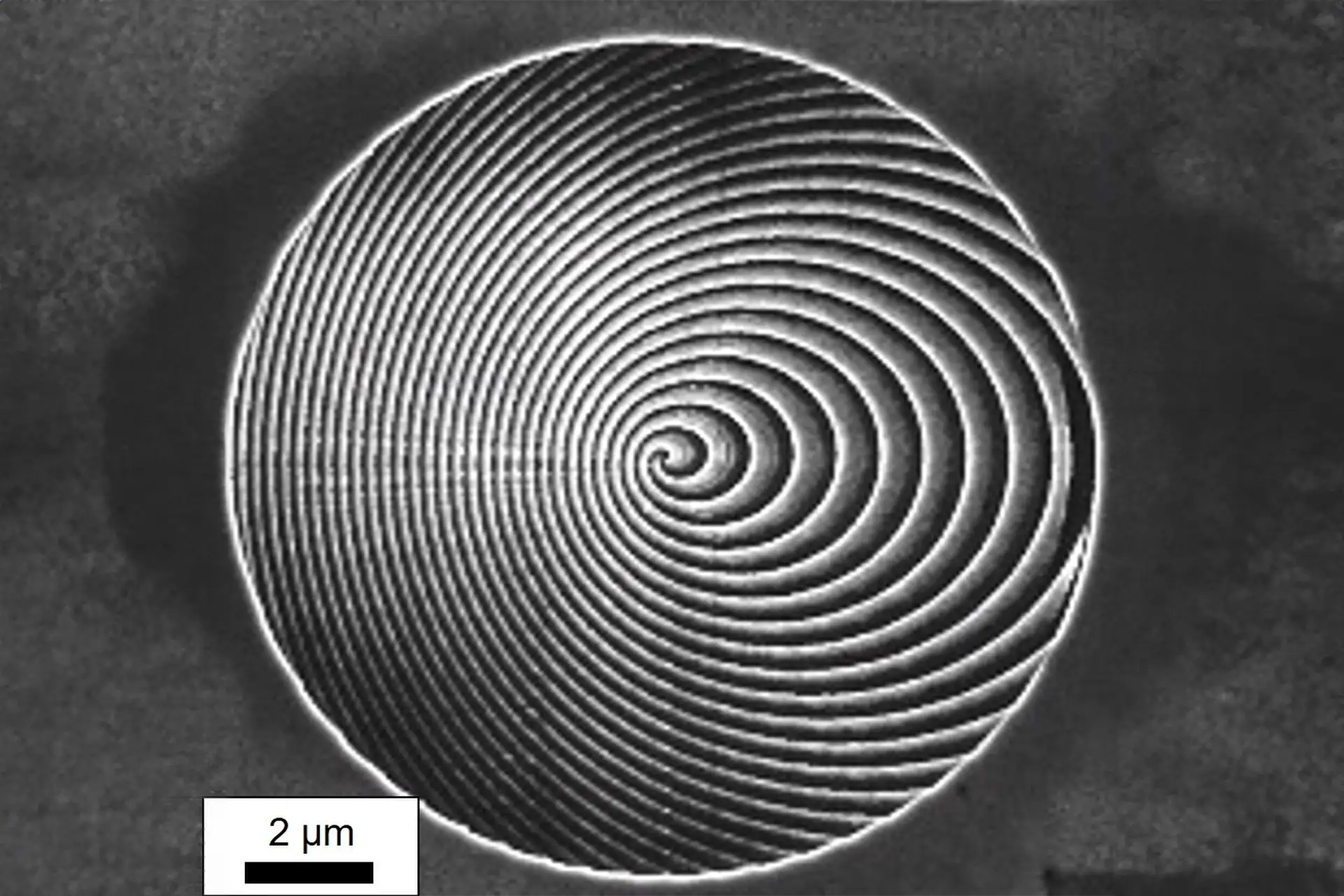
DWL 66+: Confocal microscope image of a convex fresnel lens (diameter 506 µm, height 10 µm).
Nano structured phase masks made of Silicon-nitride using thermal scanning probe lithography combined with etching. This phase mask offers the intriguiging possibilities in electron-beam shaping. (NanoFrazor)
DWL 66+: Micrograph showing the image of a Fresnel lens (diameter 506 µm, height 10 µm).
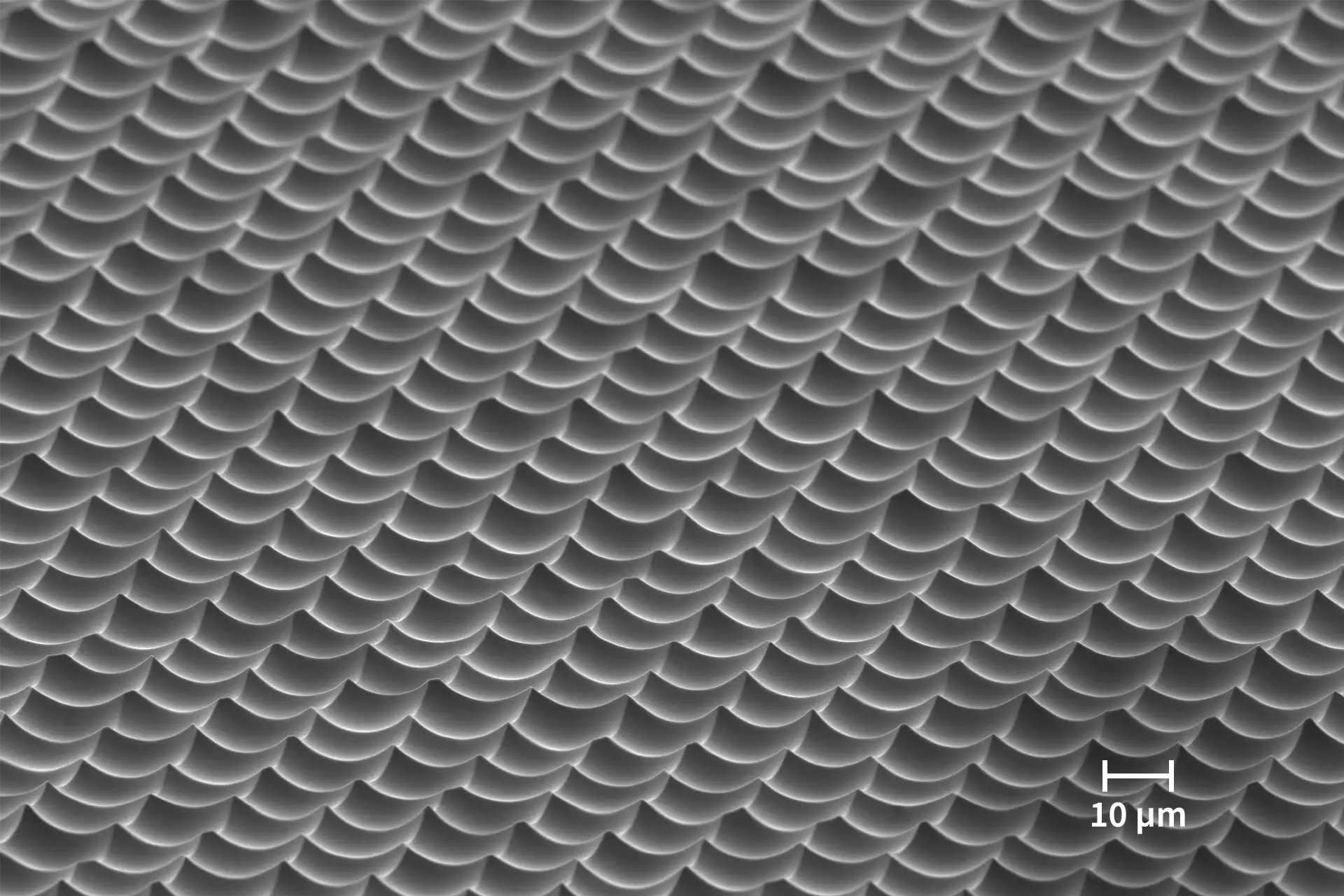
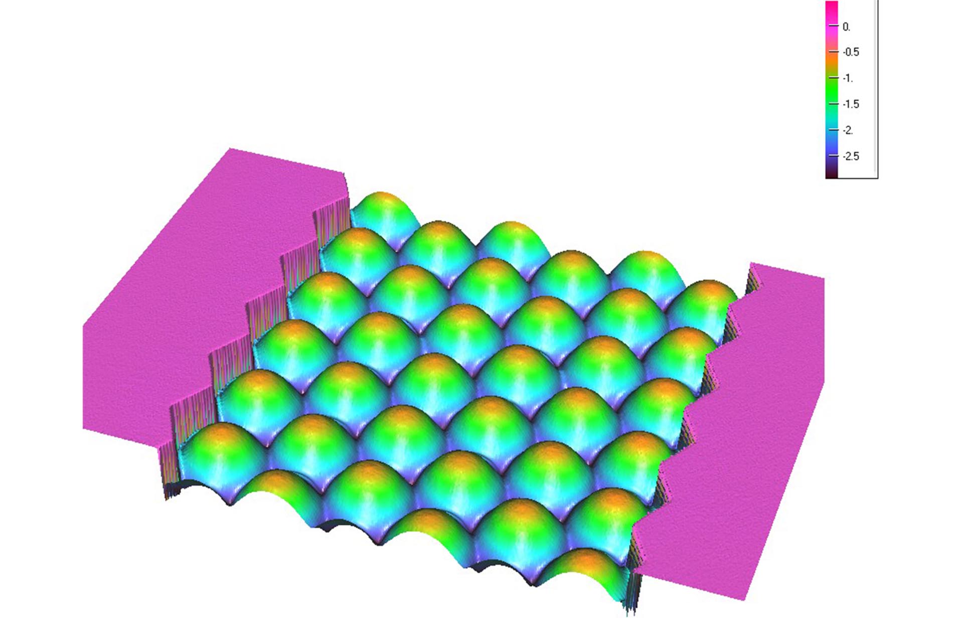
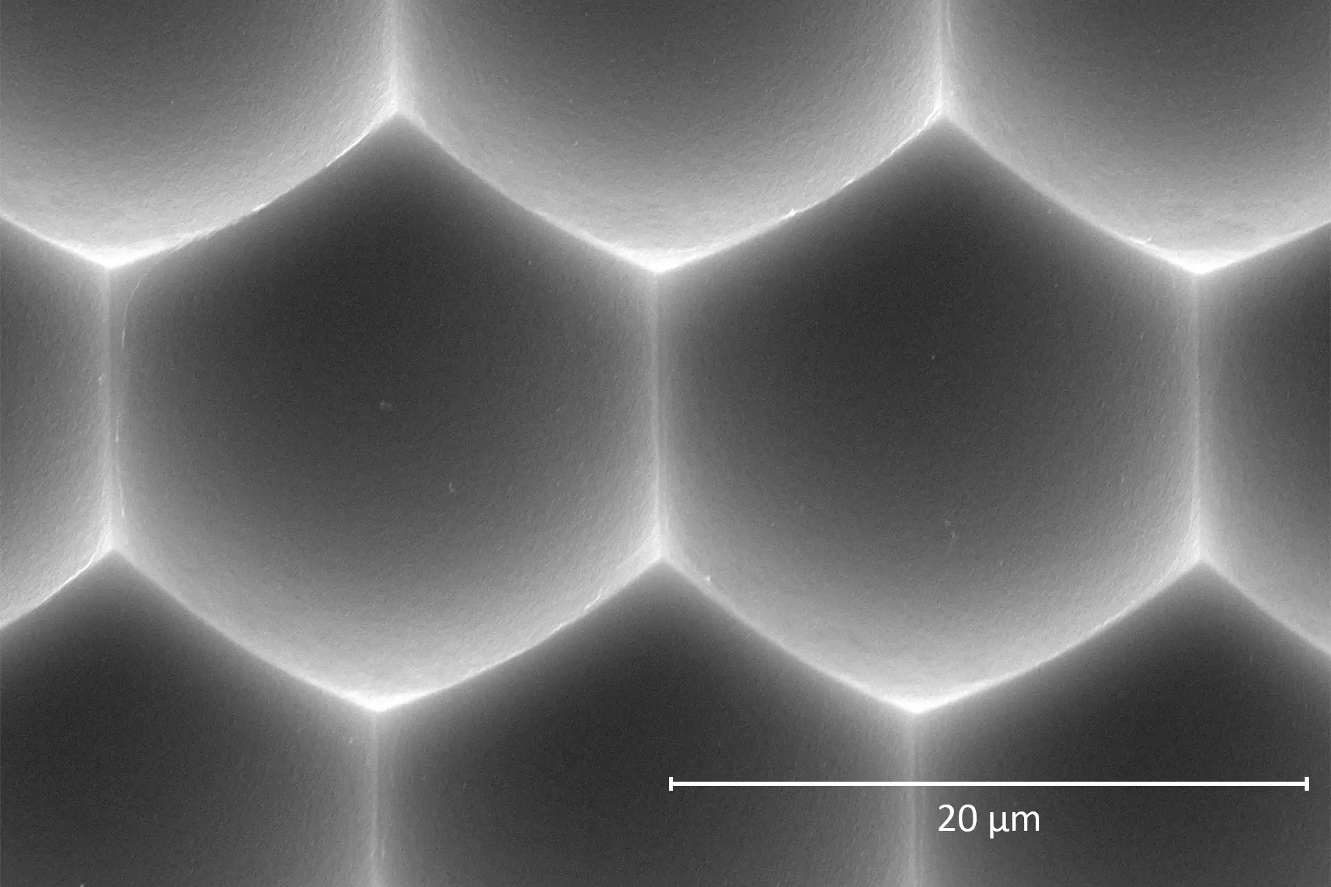
DWL 66+: Confocal microscope image of a micro lens array in a honeycomb arrangement (hexagon radius 10 µm, height 2.7 µm).
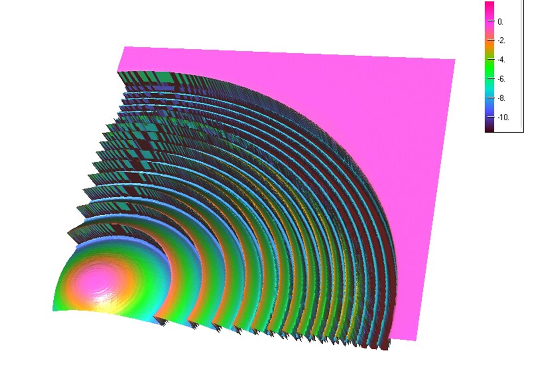
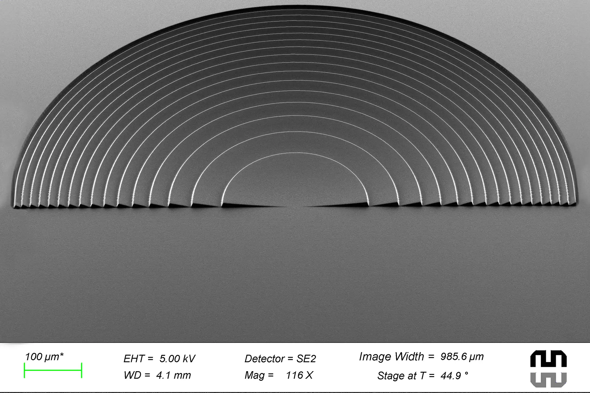
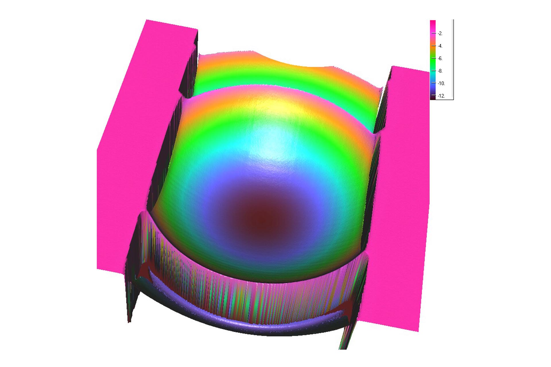
Half of a Concave Fresnel Lens,also showing its profile, Radius of curvature 840 µm, Height 10 µm, effective diameter 1mm. (DWL66+ WM III)
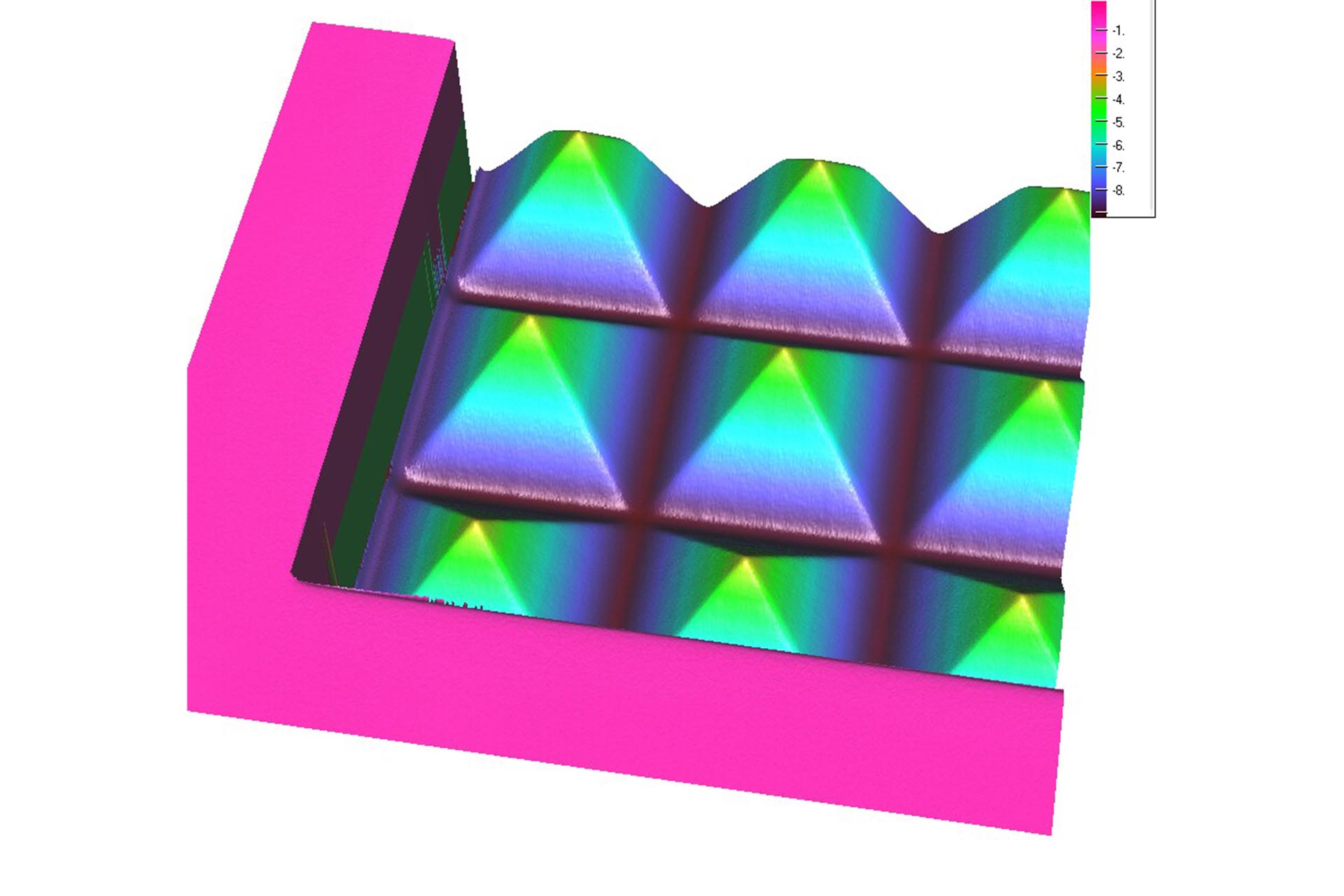
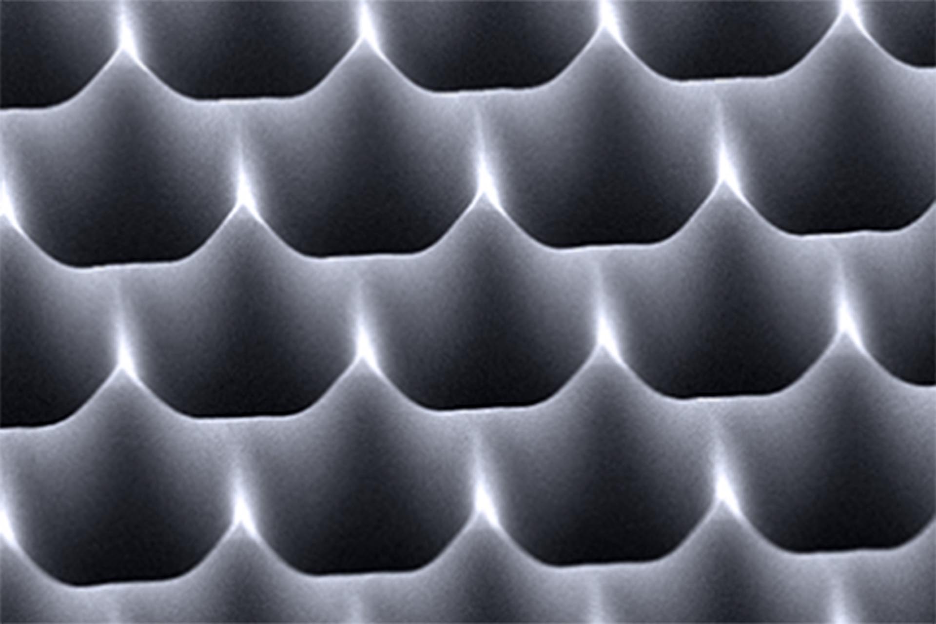
DWL 66+: Confocal microscope image of a pyramid (pitch 47 µm, height 5.8 µm).
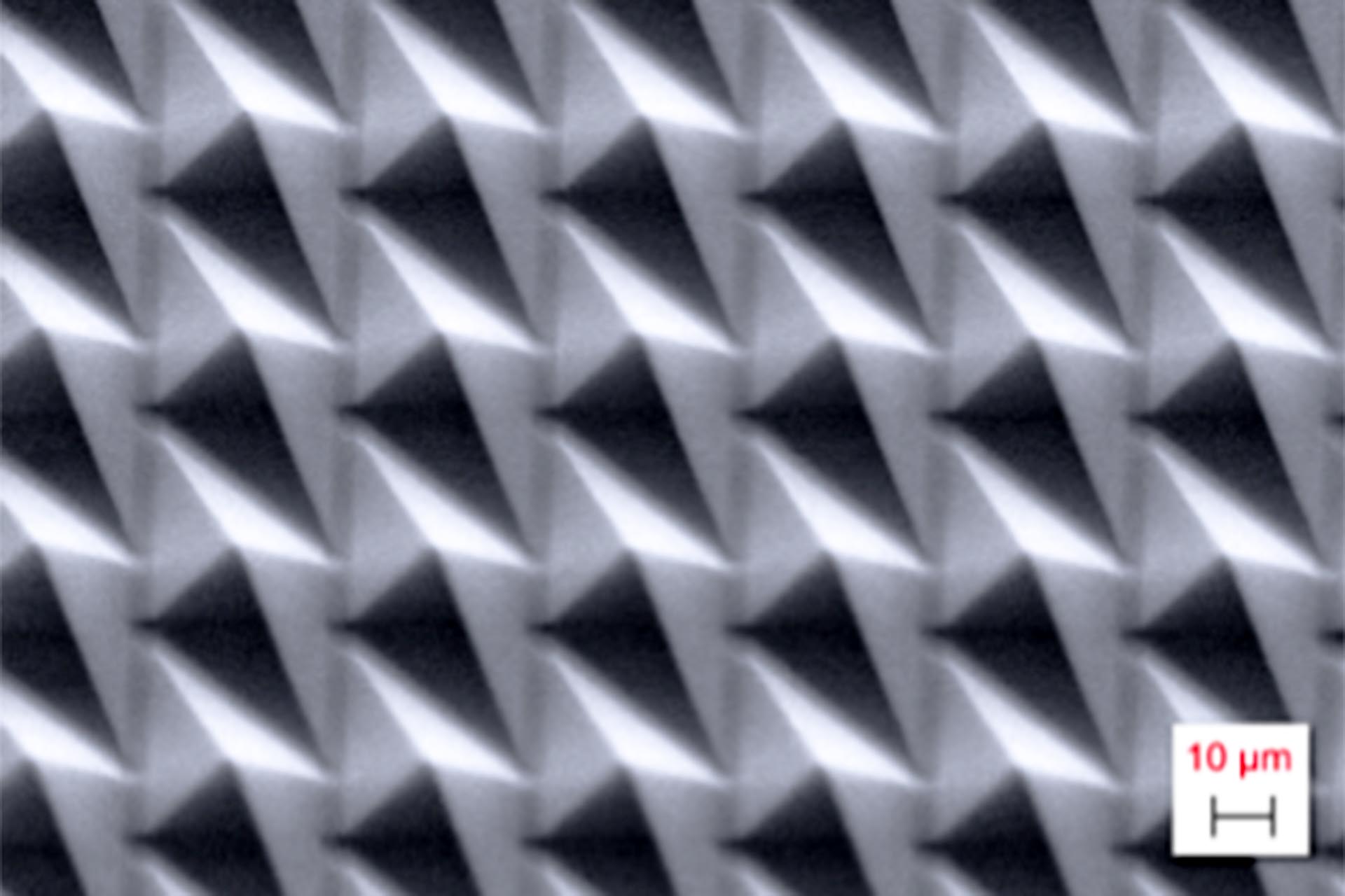
DOE square size 1µm 4steps 800nm total height View 70° x5000 (DWL66+ HiRes) Multi-level Diffractive Optical Elements (DOEs) are valuable devices commonly used for light modulation. By changing the phase profile of a laser beam, DOEs can split and shape the beam in well-defined ways, enabling the efficient generation of beam arrays or complex light patterns.
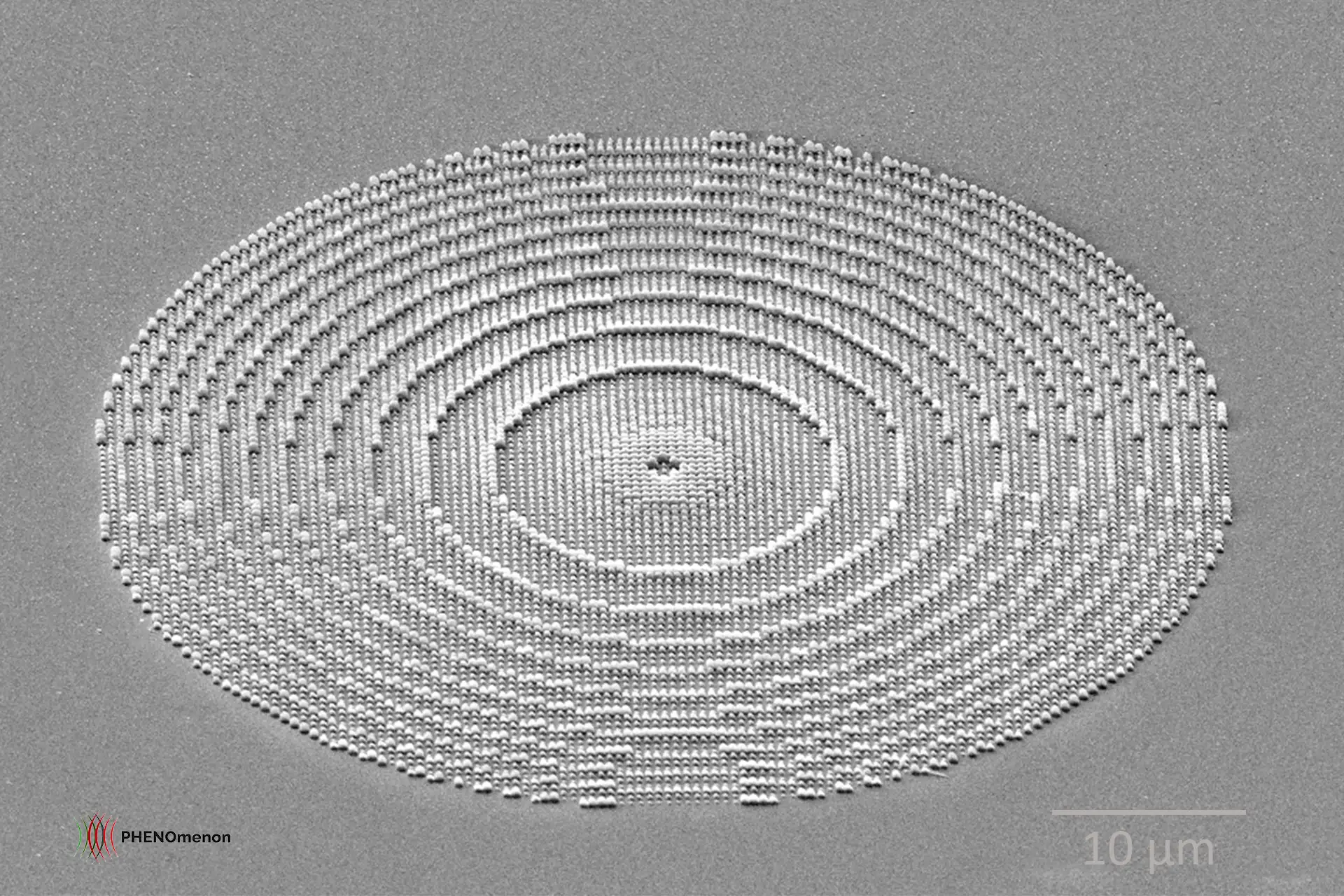
Photonic sieve made with a NanoFrazor.
A Photonic Sieve focuses light through diffraction and interference using a flat material filled with pinholes, achieving sharper focus than a Fresnel Zone plate.
DWL 66+: Confocal microscope image of the central part of a concave fresnel lens (diameter of the central part: 120 µm, height 11 µm).
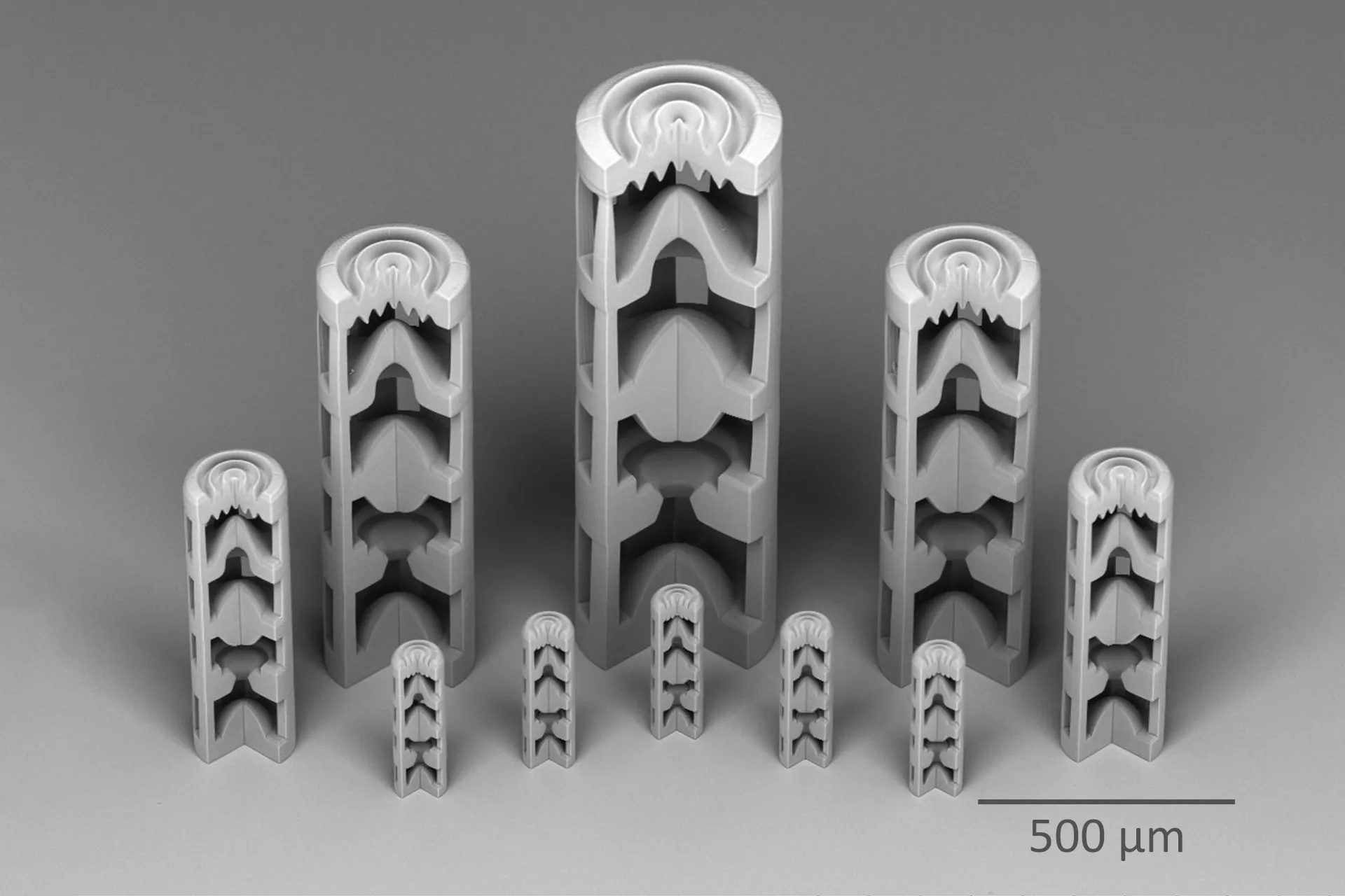
Lens stacks for applications in endoscopy (Life Sciences/Biomedical Engineering). Novel designs can be fabricated in a single process
step without the need for alignment and assembly. Fabricated with MPO 100.
Tailored diffusers and reflectors have applications for example in light sources and illumination, for example backlight units in LCD displays. This example shows a retro-reflector structure.
(Courtesy of karmic.ch)
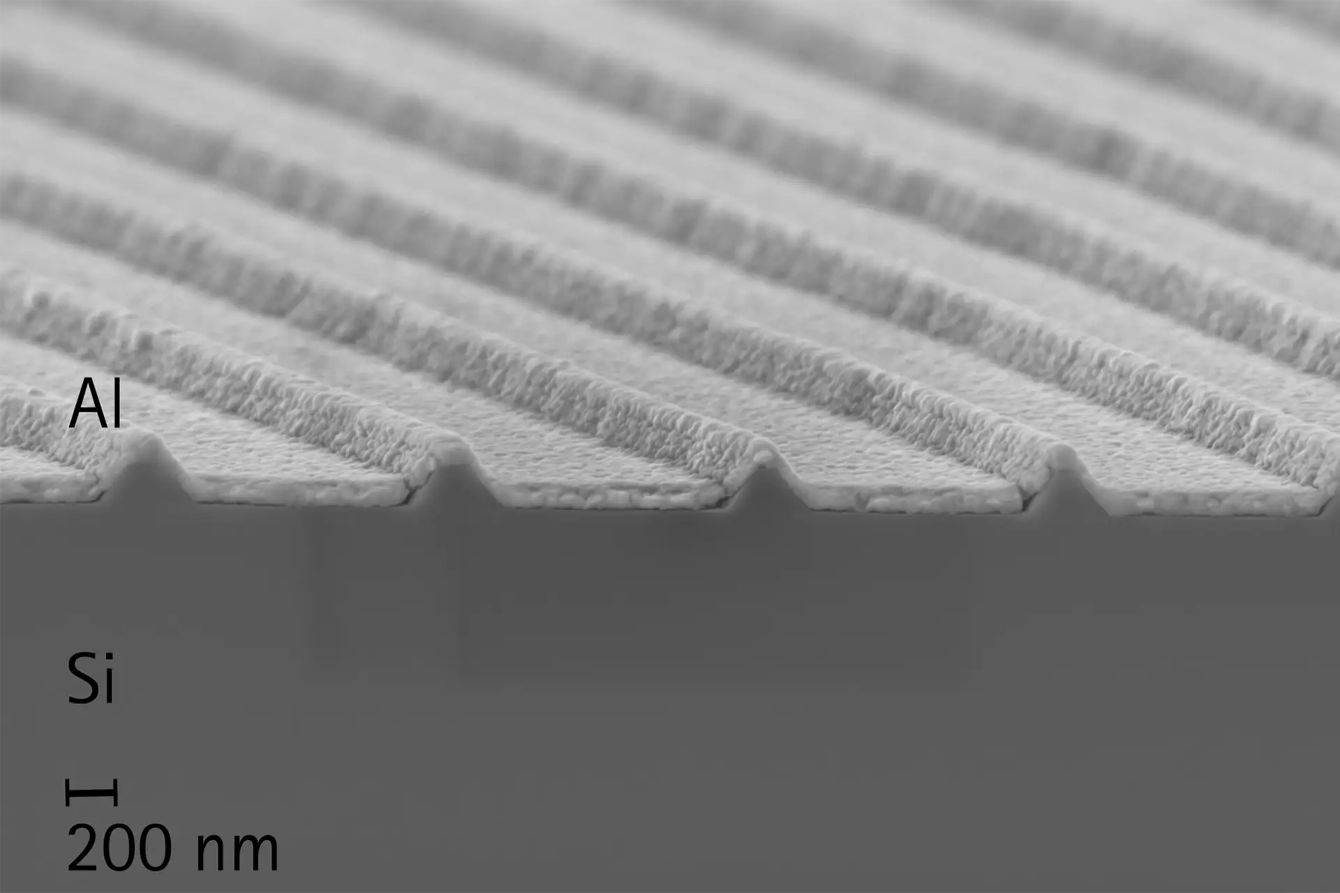
1100nm pitch grating etched in Si and coated with Al - integrated nanostructured optical reflection gratings on atom chips for quantum applications like gravimeters. (Courtesy of Sascha de Wall, IMPT)
Concave Micro lenses made in ma-P1275G. Microlenses and microlens arrays are key components in modern-day micro-optics. They are used in wavefront sensors, for fiber coupling, or for homogenizing light sources.
Microlenses written in 15 μm thick AZ4562, with a pitch of 30 μm and a radius of curvature of 16 μm.
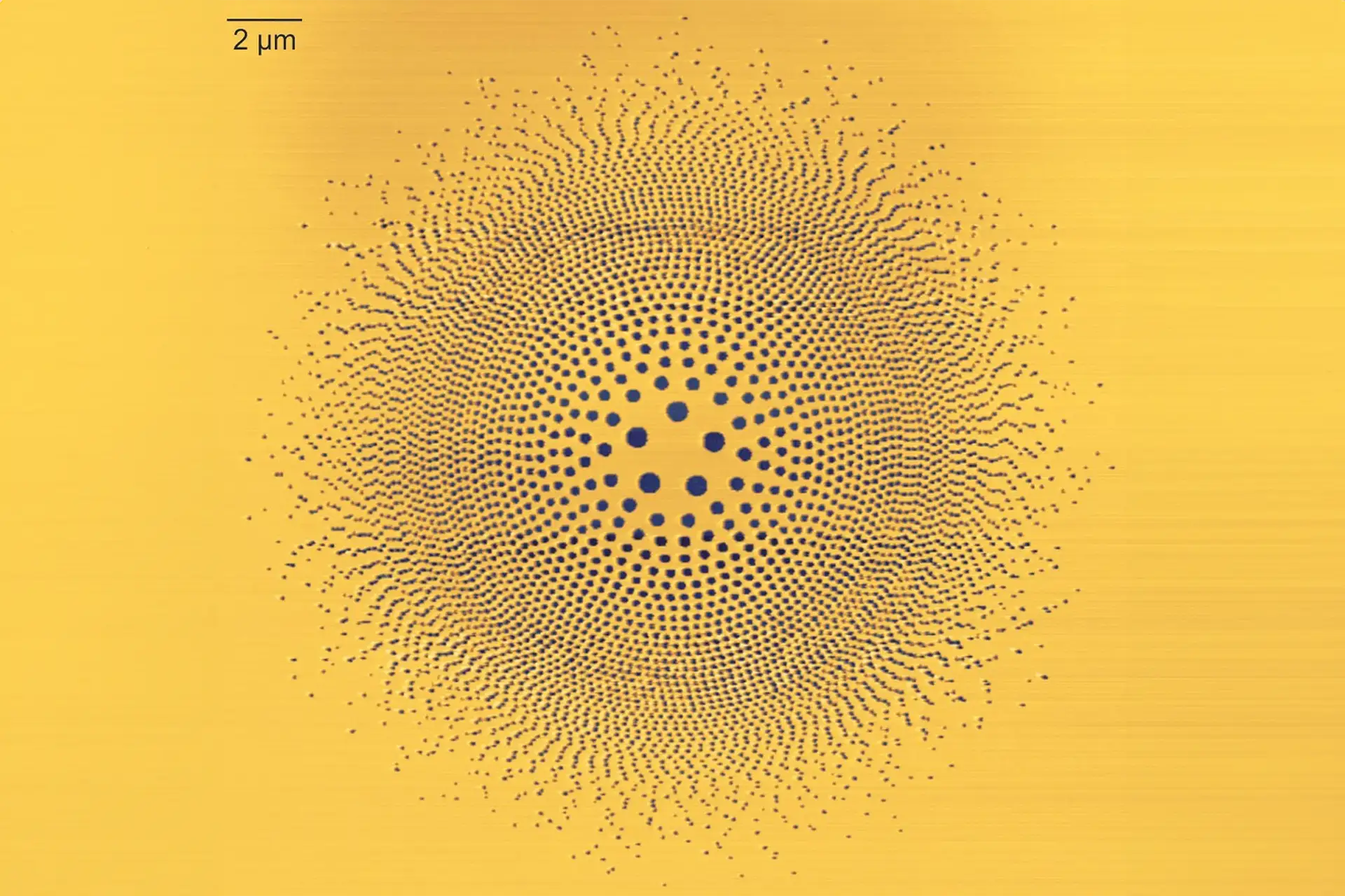
This example shows a compound structure – a complex structure made of micro- and nanostructures. The insect eye, for instance (in particular the moth- or fly-eye), consists of a series of compound structures.
(Courtesy of ShenZhen Nahum-Eli Optical Technology Inc.)
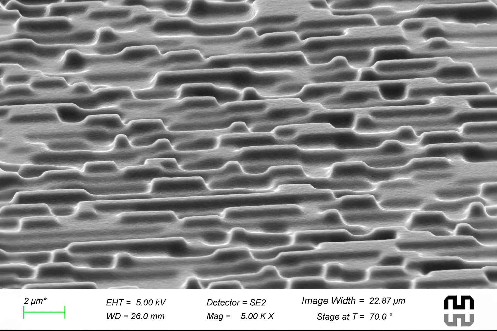
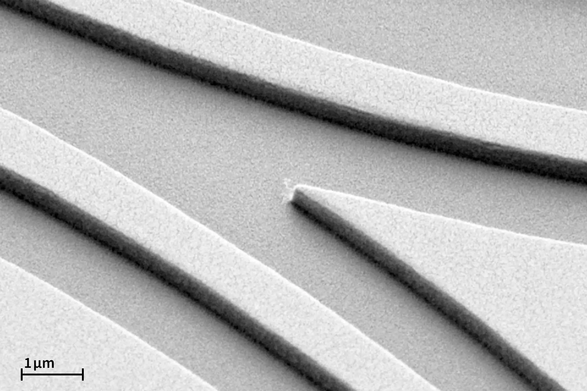
Parts of a waveguide (1 µm wide) made with a VPG 300 DI. Waveguides can guide electromagnetic waves, essential in applications like optical communication and sensors. (Courtesy of IMS Chips)
Metalens with feature sizes down to 100 nm, fabricated with MPO 100 predecessor LithoProf3D.
(Courtesy of PHENOmenon, EU-funded project, GA 780278)
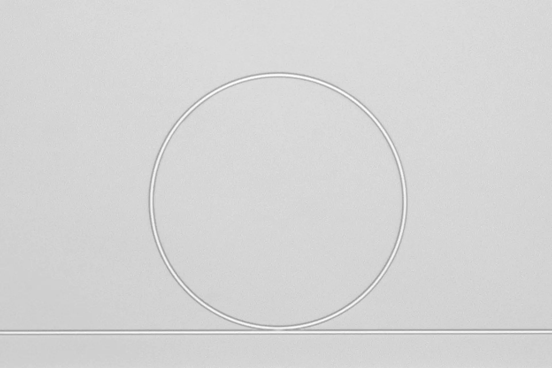
A ring resonator consists of a closed loop or ring made from a waveguide. Light is coupled into and out of the ring through waveguide arms. The geometry of the ring allows it to support resonant modes. Here the lines are 2µm wide, the distance between the line and the ring is 500 nm.
suitable Systems
DWL 66+
Direct Write Laser Lithography System
Our most versatile system for research and prototyping with variable resolution and wide selection of options.
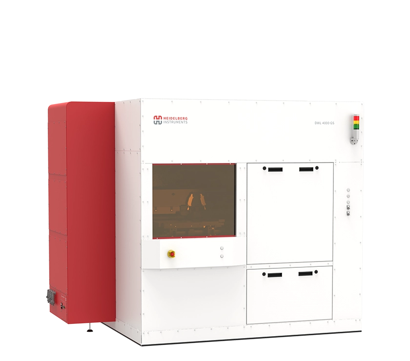
DWL 2000 GS / DWL 4000 GS
Direct Write Laser Lithography System
The most advanced industrial grayscale lithography tool on the market.
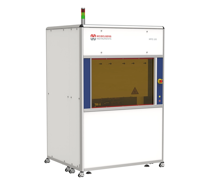
MPO 100
Two-Photon Polymerization Multi-User Tool
Multi-User Tool for 3D Lithography and 3D Microprinting of microstructures with applications in micro-optics, photonics, micro-mechanics and biomedical engineering.
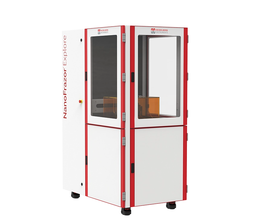
NanoFrazor Explore
Thermal Scanning Probe Lithography System
Thermal scanning probe lithography tool with direct laser sublimation and grayscale modules. Excellent alternative to e-beam lithography tools.