MEMS
Flexible Small Batch Production
-
Description
-
MEMS, short for Micro-Electro-Mechanical Systems, are microsystem components that range in size from 1 µm to 100 µm. These tiny devices enable the miniaturization of existing devices, provide new functionality using physical principles not available at the macroscale, and facilitate the development of tools that operate in the microworld. MEMS can appear as complex machines such as sensors and actuators or as simple structures like cantilevers, gearwheels, or other mechanical parts.
MEMS are used in a wide variety of applications, including accelerometers, gyroscopes, pressure sensors, biosensors, micropumps, microvalves, and many more. MOEMS, or Micro-Optical-Electro-Mechanical Systems, are a deviation from standard MEMS that combines micro-optics with other MEMS components. Examples of MOEMS include optical switches, optical modulators, and optical interconnects.
MEMS fabrication relies on the utilization of semiconductor process technology, which includes layer deposition, photolithographic patterning, and etching techniques to achieve the desired device shape. Two-Photon Polymerization can also be employed for the fabrication of certain types of MEMS or MOEMS.
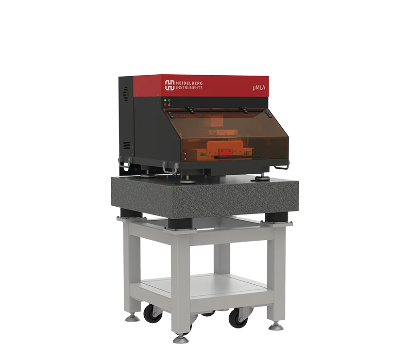
Direct Write Lithography is a highly flexible technique for modifying and shaping materials at the nano- and micro-scale. Heidelberg Instruments’ DWL and MLA series of Direct Write Laser Lithography tools can be used to create etch masks on silicon, high aspect ratio structures in thick photoresists, and material deposition in cleared resist patterns. Furthermore, the MPO 100 system offers the capability to manufacture microstructures directly in polymer materials, allowing for the creation of intricate 3D micro-mechanisms or the connection of two optical elements. Visit the corresponding product pages to find out more (see below).
-
Requirements
-
Rapid prototyping
Various structure shapes and dimensions
Throughput independent of pattern complexity
-
Solutions
-
High throughput
Exposure speeds up to 5000 mm²/minGrayscale lithography (DWL series)
Used to pattern both simple or complex 2.5D topographies (e.g., tapered channels)High aspect ratio
Tall structures up to 1mm in heightNo undercut
The structures can be used for replication
MEMS, short for Micro-Electro-Mechanical Systems, are microsystem components that range in size from 1 µm to 100 µm. These tiny devices enable the miniaturization of existing devices, provide new functionality using physical principles not available at the macroscale, and facilitate the development of tools that operate in the microworld. MEMS can appear as complex machines such as sensors and actuators or as simple structures like cantilevers, gearwheels, or other mechanical parts.
MEMS are used in a wide variety of applications, including accelerometers, gyroscopes, pressure sensors, biosensors, micropumps, microvalves, and many more. MOEMS, or Micro-Optical-Electro-Mechanical Systems, are a deviation from standard MEMS that combines micro-optics with other MEMS components. Examples of MOEMS include optical switches, optical modulators, and optical interconnects.
MEMS fabrication relies on the utilization of semiconductor process technology, which includes layer deposition, photolithographic patterning, and etching techniques to achieve the desired device shape. Two-Photon Polymerization can also be employed for the fabrication of certain types of MEMS or MOEMS.
Direct Write Lithography is a highly flexible technique for modifying and shaping materials at the nano- and micro-scale. Heidelberg Instruments’ DWL and MLA series of Direct Write Laser Lithography tools can be used to create etch masks on silicon, high aspect ratio structures in thick photoresists, and material deposition in cleared resist patterns. Furthermore, the MPO 100 system offers the capability to manufacture microstructures directly in polymer materials, allowing for the creation of intricate 3D micro-mechanisms or the connection of two optical elements. Visit the corresponding product pages to find out more (see below).
Rapid prototyping
Various structure shapes and dimensions
Throughput independent of pattern complexity
High throughput
Grayscale lithography (DWL series)
High aspect ratio
No undercut
Application images


suitable Systems
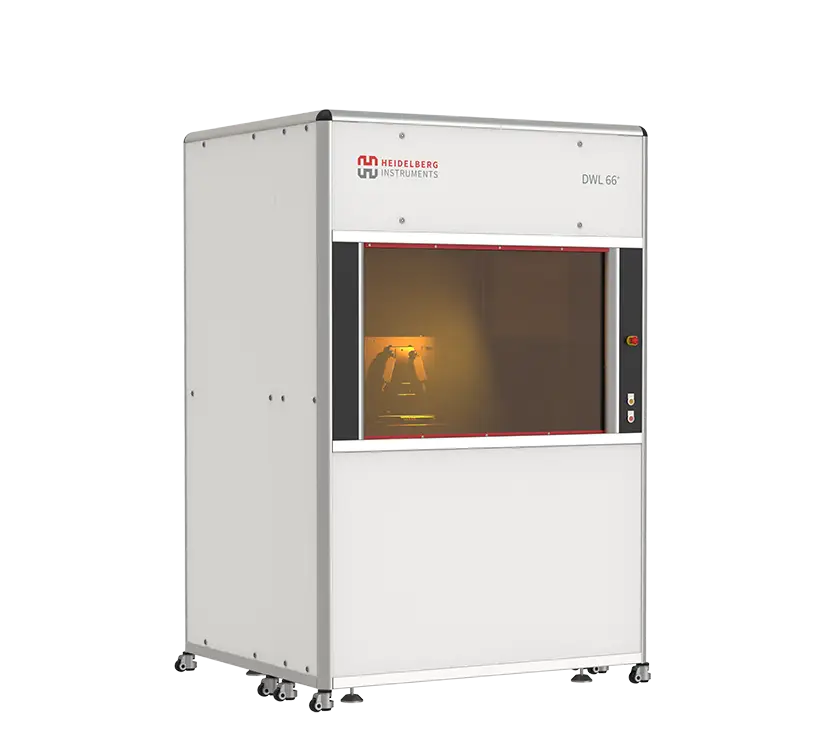
DWL 66+
- Direct Write Laser Lithography System
Our most versatile system for research and prototyping with variable resolution and wide selection of options.
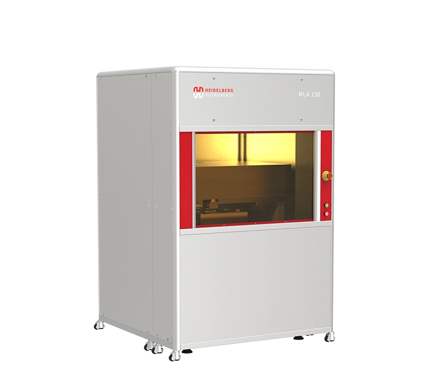
MLA 150
- Maskless Aligner
The fastest maskless tool for rapid prototyping, the alternative to the mask aligners. Perfect for standard binary lithography.
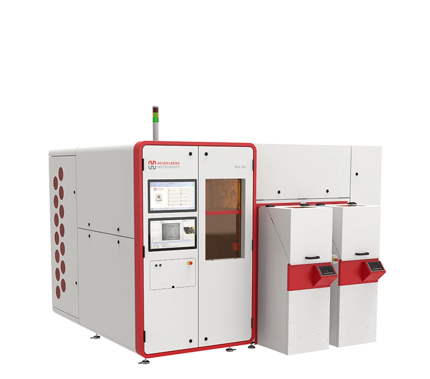
MLA 300
- Maskless Aligner
Optimized for industrial production with highest throughput and seamless integration into industrial production lines.
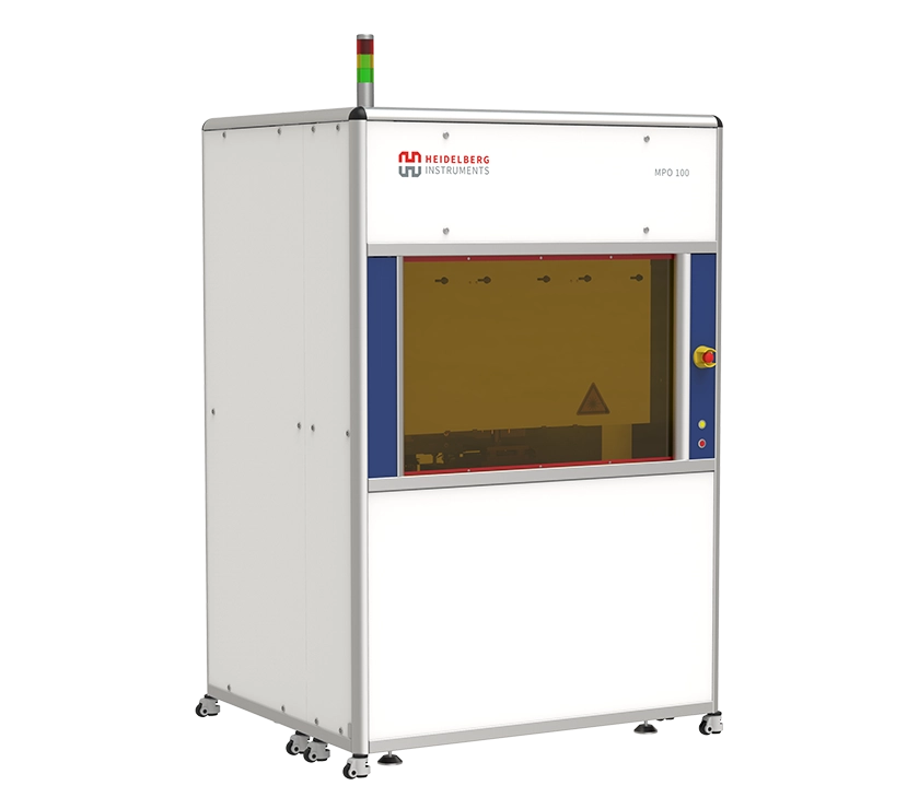
MPO 100
- Two-Photon Polymerization Multi-User Tool
Multi-User Tool for 3D Lithography and 3D Microprinting of microstructures with applications in micro-optics, photonics, micro-mechanics and biomedical engineering.
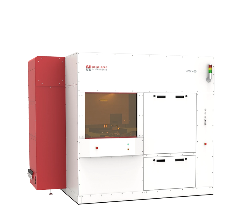
VPG+ 200 / VPG+ 400
- Volume Pattern Generator
A production tool for standard photomasks and microstructures in i-line resists.
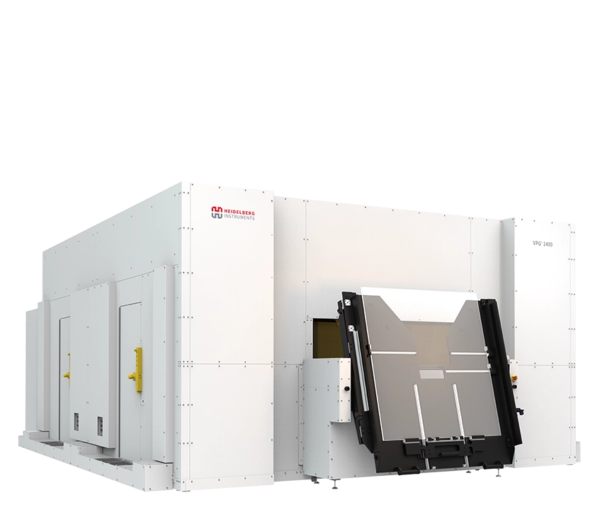
VPG+ 800 / VPG+ 1400
- Volume Pattern Generator
Photomask production on large substrates, perfect for display applications.

