Conventional lithography processes require wet development of the resist before the written features can be inspected and measured.
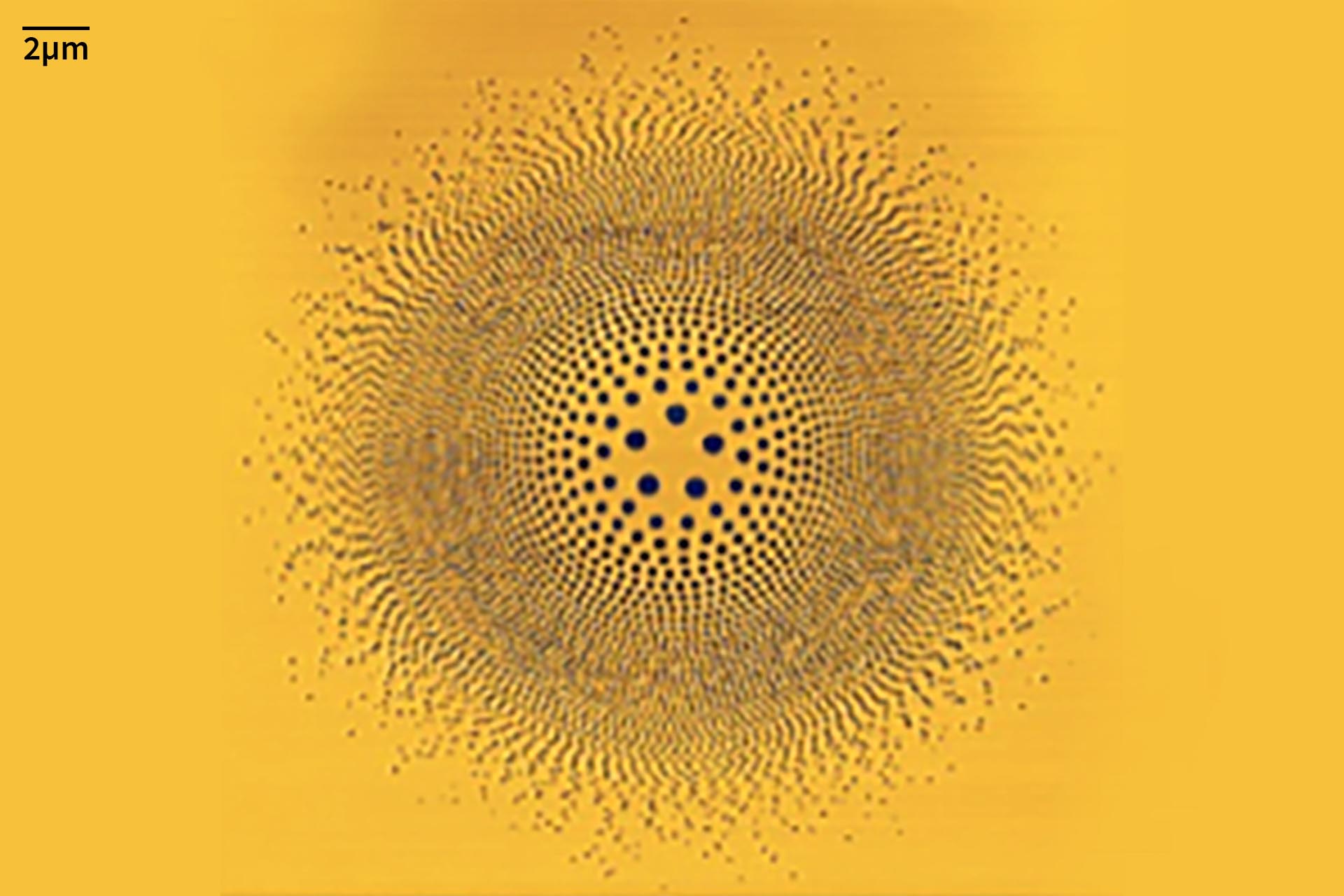
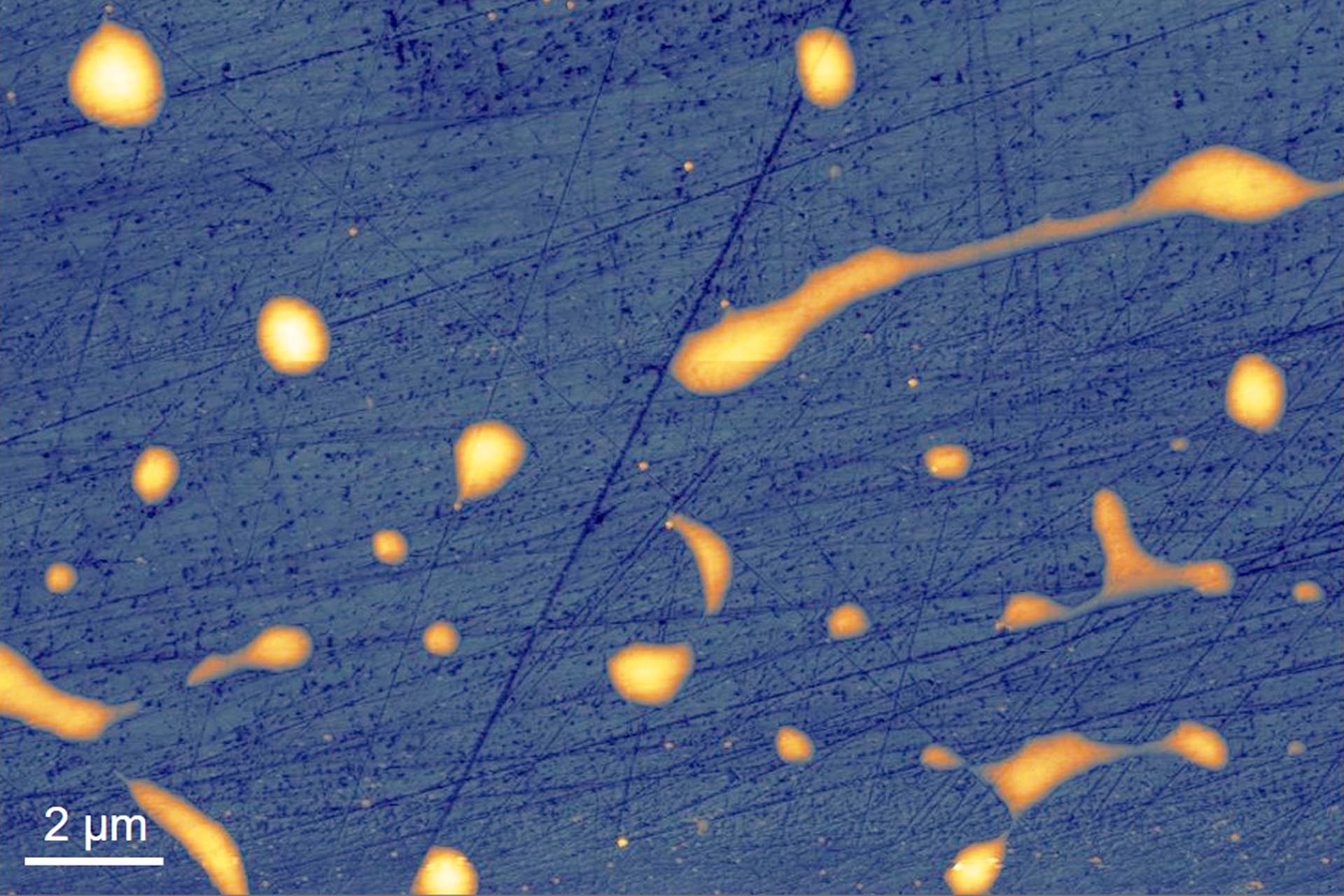
Direct-write lithography processes such as NanoFrazor lithography and low-throughput laser writing directly sublimate thermal resists like PPA. This direct removal of resist enables immediate inspection and metrology of the written features, which is beneficial for process development and rapid turnaround fabrication. Furthermore, it allows the NanoFrazor tools to achieve and maintain extremely high patterning quality by the patented “Closed-Loop Lithography” approach.
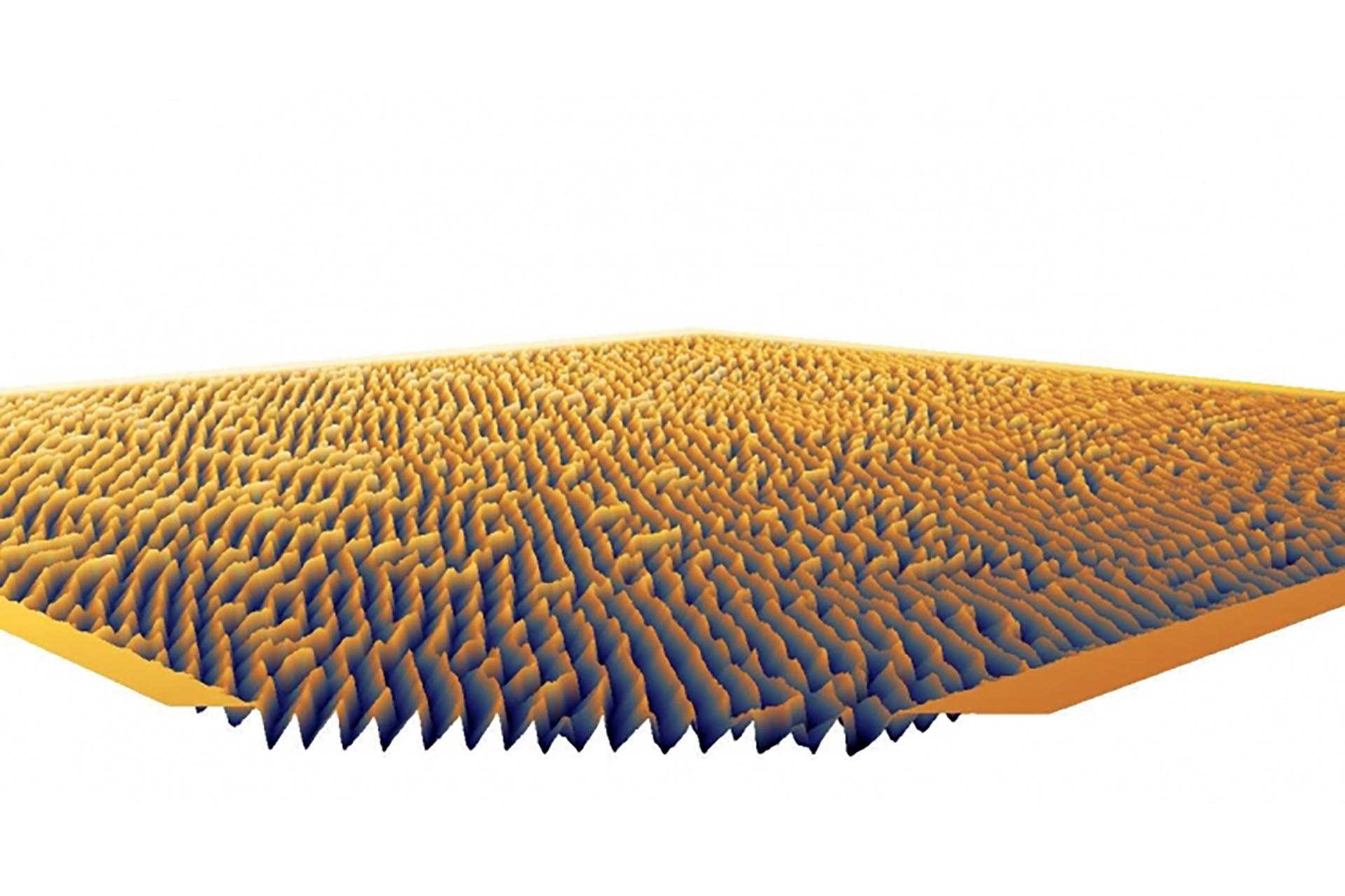
The NanoFrazor systems use the same tip that is used for patterning for in-situ inspection of the written structures. Topography is imaged by means of a special metrology technique, which originates from the discovery of the Nobel Prize winner Gerd Binnig that the electrical resistance of the IBM Millipede cantilevers was strongly distance-dependent. This discovery enabled the easy-to-use and reliable NanoFrazor distance sensing method, enabling fast imaging and accurate metrology of high-resolution, shallow topographies in soft surfaces (like resist coatings).