Thermal scanning probe lithography tool with a hybrid direct laser sublimation and grayscale patterning capability
-
Product Description
-
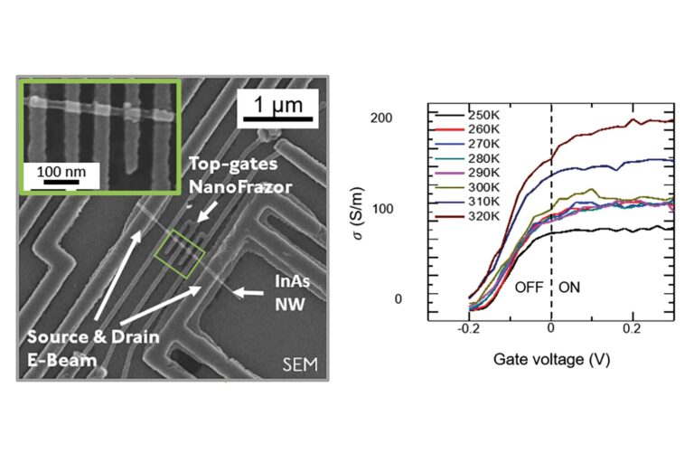
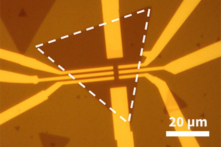
The NanoFrazor Explore is the first commercial Thermal Scanning probe Lithography System. The NanoFrazor Explore can be used in various application areas, such as quantum devices, 1D/2D materials like quantum dots, Dolan bridges and Josephson junctions, and nanoscale arrays. The unique capabilities of the NanoFrazor Explore enable novel research in both new devices and new materials. For example, Thermal Scanning Probe Lithography can be used in advanced applications such as grayscale photonics devices, nanofluidic structures or biomimetic substrates for cell growth, or any application requiring local modification of materials via heat, e.g., chemical reactions and physical phase changes.
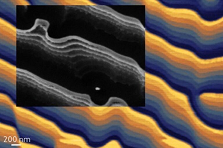
With the direct laser sublimation module, nano- and micro-structures are now seamlessly and quickly written into the same resist layer in a single fabrication step. In-situ imaging enables two unique features: markerless overlay and comparison of the written and target patterns during writing, in such a way that the parameters can be immediately adjusted. This approach, called closed-loop lithography, results in sub-2 nm vertical precision for 2.5D (grayscale) shapes of any complexity. Fast and precise control of a heated nanoscale tip enables innovation not otherwise feasible with other techniques.
The technology behind the system is the result of more than 20 years of intensive research and development (R&D) that started at IBM Research Zürich, and now takes place at Heidelberg Instruments Nano. The NanoFrazo hardware and software are constantly advancing to extend the capabilities and performance of the tool and the wide range of applications. Our dedicated team of experts continues to develop and optimize the pattern transfer processes for different applications. We compile this know-how in a growing library of best practices and protocols to support our customers.
The NanoFrazor Explore is the first commercial Thermal Scanning probe Lithography System. The NanoFrazor Explore can be used in various application areas, such as quantum devices, 1D/2D materials like quantum dots, Dolan bridges and Josephson junctions, and nanoscale arrays. The unique capabilities of the NanoFrazor Explore enable novel research in both new devices and new materials. For example, Thermal Scanning Probe Lithography can be used in advanced applications such as grayscale photonics devices, nanofluidic structures or biomimetic substrates for cell growth, or any application requiring local modification of materials via heat, e.g., chemical reactions and physical phase changes.
With the direct laser sublimation module, nano- and micro-structures are now seamlessly and quickly written into the same resist layer in a single fabrication step. In-situ imaging enables two unique features: markerless overlay and comparison of the written and target patterns during writing, in such a way that the parameters can be immediately adjusted. This approach, called closed-loop lithography, results in sub-2 nm vertical precision for 2.5D (grayscale) shapes of any complexity. Fast and precise control of a heated nanoscale tip enables innovation not otherwise feasible with other techniques.
The technology behind the system is the result of more than 20 years of intensive research and development (R&D) that started at IBM Research Zürich, and now takes place at Heidelberg Instruments Nano. The NanoFrazo hardware and software are constantly advancing to extend the capabilities and performance of the tool and the wide range of applications. Our dedicated team of experts continues to develop and optimize the pattern transfer processes for different applications. We compile this know-how in a growing library of best practices and protocols to support our customers.
-
Product Highlights
-
Thermal Scanning Probe Lithography
New approach to nanopatterning enabling applications not otherwise feasibleHigh-resolution
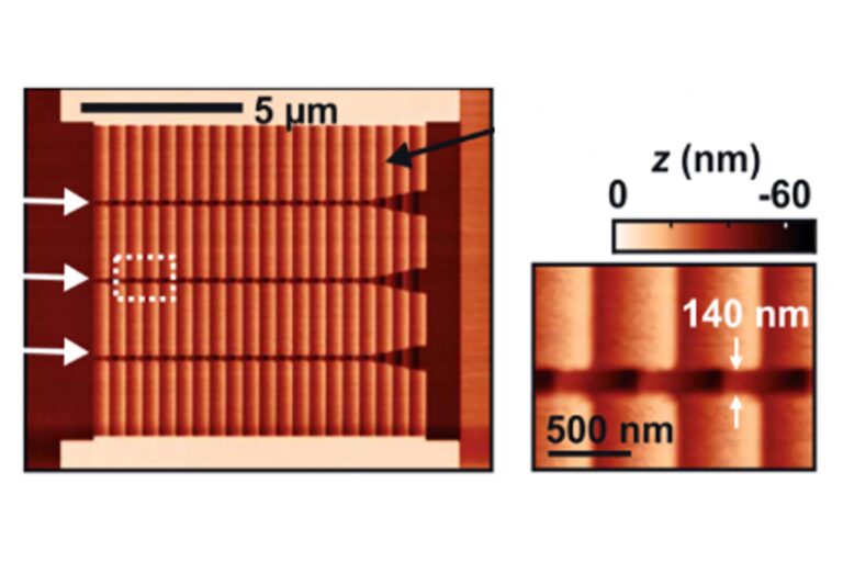
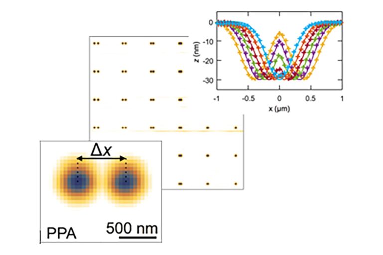
Easy patterning of nanostructures even with complex geometries; minimum lateral features 15 nm, vertical resolution 2 nmDamage-free Lithography
No damage from charged particles, no proximity effects, clean lift-offCompatibility
With all standard pattern transfer methods: lift-off, etching, etc. – knowledge resource and best practices available in our “Recipe Book”Unique Thermal Cantilevers
Integrated microheater and distance sensor for easy exchange and cost-effectivenessPrecise Overlay and Stitching
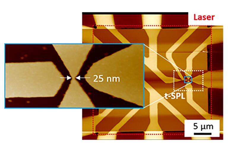
Markerless overlay and stitching accuracy 25 nm specified, sub-10 nm overlay shownIn-situ Imaging
Real-time visualization of patterned structure propertiesLaser Sublimation Module
High-throughput exposure of coarse structures in the same exposure step; 405 nm wavelength CW fiber laserCompact
1850 mm x 780 mm x 1280 mmVibration Isolation
Three-layer acoustic and superior vibration isolation (>98% @ 10 Hz)Low Cost of Ownership
No need for a cleanroom, vacuum pump or expensive consumables -
Available Modules
-
Grayscale Software Module
2.5D patterning at <2 nm vertical resolutionGlovebox Integration
Customized solution ensures minimized contamination for work in controlled environments
The NanoFrazor Explore is the first commercial Thermal Scanning probe Lithography System. The NanoFrazor Explore can be used in various application areas, such as quantum devices, 1D/2D materials like quantum dots, Dolan bridges and Josephson junctions, and nanoscale arrays. The unique capabilities of the NanoFrazor Explore enable novel research in both new devices and new materials. For example, Thermal Scanning Probe Lithography can be used in advanced applications such as grayscale photonics devices, nanofluidic structures or biomimetic substrates for cell growth, or any application requiring local modification of materials via heat, e.g., chemical reactions and physical phase changes.
With the direct laser sublimation module, nano- and micro-structures are now seamlessly and quickly written into the same resist layer in a single fabrication step. In-situ imaging enables two unique features: markerless overlay and comparison of the written and target patterns during writing, in such a way that the parameters can be immediately adjusted. This approach, called closed-loop lithography, results in sub-2 nm vertical precision for 2.5D (grayscale) shapes of any complexity. Fast and precise control of a heated nanoscale tip enables innovation not otherwise feasible with other techniques.
The technology behind the system is the result of more than 20 years of intensive research and development (R&D) that started at IBM Research Zürich, and now takes place at Heidelberg Instruments Nano. The NanoFrazo hardware and software are constantly advancing to extend the capabilities and performance of the tool and the wide range of applications. Our dedicated team of experts continues to develop and optimize the pattern transfer processes for different applications. We compile this know-how in a growing library of best practices and protocols to support our customers.
Thermal Scanning Probe Lithography
High-resolution
Damage-free Lithography
Compatibility
Unique Thermal Cantilevers
Precise Overlay and Stitching
In-situ Imaging
Laser Sublimation Module
Compact
Vibration Isolation
Low Cost of Ownership
Grayscale Software Module
Glovebox Integration
Customer applications
Why customers choose our systems
Xiaorui Zheng, Assistant Professor, Principal Investigator
Westlake University
Hangzhou, China
Technical Data
| Thermal Probe Writing | Direct Laser Sublimation | |
|---|---|---|
| Patterning performance | ||
| Minimum structure size [nm] | 15 | 600 |
| Minimum Lines and Spaces [half pitch, nm] | 25 | 1000 |
| Grayscale / 2.5D-resolution (step size in PPA) [nm] | 2 | - |
| Writing field size [X μm x Y μm] | 60 x 60 | 60 x 60 |
| Field stitching accuracy (markerless, using in-situ imaging) [nm] | 25 | 600 |
| Overlay accuracy (markerless, using in-situ imaging) [nm] | 25 | 600 |
| Write speed (typical scan speed) [mm/s] | 1 | 5 |
| Write speed (50 nm pixel) [μm²/min] | 1000 | 100000 |
| Topography performance | ||
| Lateral imaging resolution (feature size) [nm] | 10 | 10 |
| Vertical resolution (topography sensitivity) [nm] | <0.5 | <0.5 |
| Imaging speed (@ 50 nm resolution) [μm²/min] | 1000 | 1000 |
| System features | |
|---|---|
| Substrate sizes | 1 x 1 mm² to 100 x 100 mm² (150 x 150 mm² possible with limitations) Thickness: 10 mm with optical access, 15 mm without optical access. |
| Optical microscope | 0.6 μm digital resolution, 2 μm diffraction limit, 1.0 mm x 1.0 mm field of view, autofocus |
| Laser source and optics | 405 nm wavelength CW fiber laser, more than 110 mW output power on sample, 1.2 μm minimum focal spot size |
| Real-time laser autofocus | Using the distance sensor of the NanoFrazor cantilever |
| Magnetic cantilever holder | Fast (<1 min) and accurate tip exchange |
| Housing | Three-layer acoustic isolation, superior vibration isolation (>98% @ 10 Hz) PC-controlled temperature and humidity monitoring, gas-flow regulation |
| Software features | GDS and bitmap import, 0.1 nm address grid, 256 grayscale levels, topography image analysis and drawing for overlay, mix & match between tip and laser writing, fully automated calibration routines, Python scripting |
| NanoFrazor cantilever features | |
| Integrated components | Tip heater, topography sensor, electrostatic actuation |
| Tip geometry | Conical tip with <10 nm radius and 750 nm length |
| Tip heater temperature range | 25 °C – 1100 °C (<1 °C setpoint resolution) |
| System dimensions & installation requirements | |
| Height × width × depth | 1850 mm x 780 mm x 1280 mm |
| Weight | 650 kg |
| Power input | 1 x 110 or 220 V AC, 10 A |
| Gas input | Compressed air and/or nitrogen with >4 bar |
| Other considerations | |
| Recipe book with detailed descriptions of various processes is included (regularly updated with software) | |
| Cantilever tips degrade over time (>50 h patterning possible). Exchange is fast and low cost for tool owners. | |
| A clean room or special laboratory is not required. No vacuum needed. |
Please note
Specifications depend on individual process conditions and may vary according to equipment configuration. Write speed depends on pixel size and write mode. Design and specifications are subject to change without prior notice.