


Description
Semiconductors are characterized by their ability to vary their electrical conductivity when exposed to external factors like voltage, heat, or light. They serve as a foundation for electronic devices in modern technology. Semiconductor devices are constructed on wafers composed of a variety of materials. Some wafers consist of a single element, such as silicon, while others incorporate a blend of elements, forming complex crystalline structures with unique electronic properties, as seen in compound semiconductors.
Photolithography is a pivotal process in semiconductor manufacturing that utilizes masks or direct writing techniques to transfer precise patterns onto wafers. It plays a crucial role in defining the intricate structures that form the basis of integrated circuits and other semiconductor devices.
Heidelberg Instruments offers tools that are suited to several critical processes during the fabrication of semiconductor-based devices, from reticles demanding high precision and high uniformity to high-throughput maskless exposures with adaptive patterning. These laser lithography tools offer versatility by enabling direct writing on photoresist-coated surfaces, facilitating rapid prototyping and customization. Their precision in alignment supports multi-layer device production and can correct for individual die misalignment and deformation. This also makes them suitable for semiconductor packaging.
Requirements
Solutions
Semiconductors are characterized by their ability to vary their electrical conductivity when exposed to external factors like voltage, heat, or light. They serve as a foundation for electronic devices in modern technology. Semiconductor devices are constructed on wafers composed of a variety of materials. Some wafers consist of a single element, such as silicon, while others incorporate a blend of elements, forming complex crystalline structures with unique electronic properties, as seen in compound semiconductors.
Photolithography is a pivotal process in semiconductor manufacturing that utilizes masks or direct writing techniques to transfer precise patterns onto wafers. It plays a crucial role in defining the intricate structures that form the basis of integrated circuits and other semiconductor devices.
Heidelberg Instruments offers tools that are suited to several critical processes during the fabrication of semiconductor-based devices, from reticles demanding high precision and high uniformity to high-throughput maskless exposures with adaptive patterning. These laser lithography tools offer versatility by enabling direct writing on photoresist-coated surfaces, facilitating rapid prototyping and customization. Their precision in alignment supports multi-layer device production and can correct for individual die misalignment and deformation. This also makes them suitable for semiconductor packaging.
Optimized for industrial production with highest throughput and seamless integration into industrial production lines.
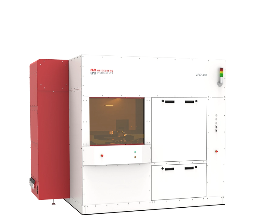
A production tool for standard photomasks and microstructures in i-line resists.
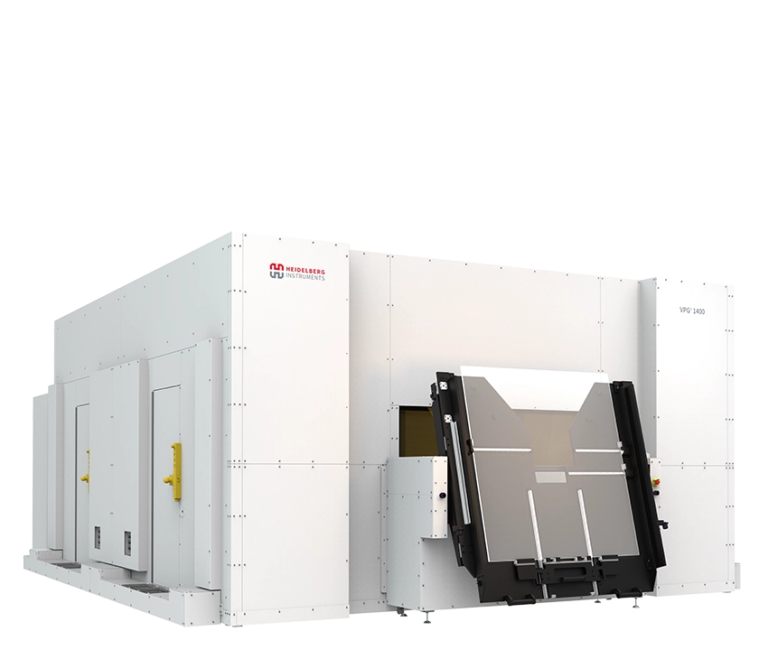
Photomask production on large substrates, perfect for display applications.
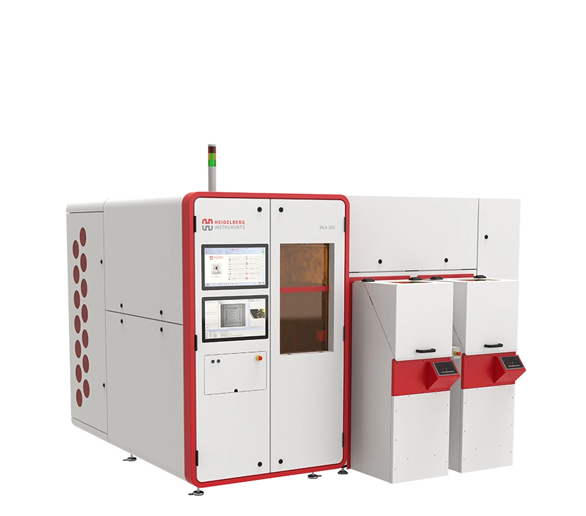
Maskless direct imager for high-accuracy and high-resolution microstructures.
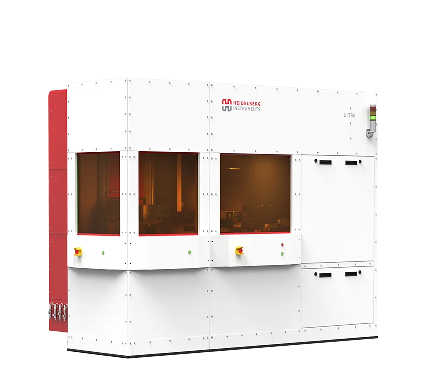
A tool specifically designed to produce mature semiconductor photomasks.
We are always at your disposal.
Please send us your request.
To view the form, please enable Marketing cookies.
Subscribe to our newsletter
to receive the newest information.
To view the form, please enable Marketing cookies.