


Description
Displays represent a fundamental component in modern electronics, providing visual interfaces for a wide range of devices, from smartphones to large-scale flat-panel displays (FPD). Display technologies depend on materials with diverse electrical conductivity, like ITO. These materials are layered onto substrates, forming the basis for pixelated displays. Utilizing photolithography, intricate patterns are transferred into these materials using masks or direct writing techniques.
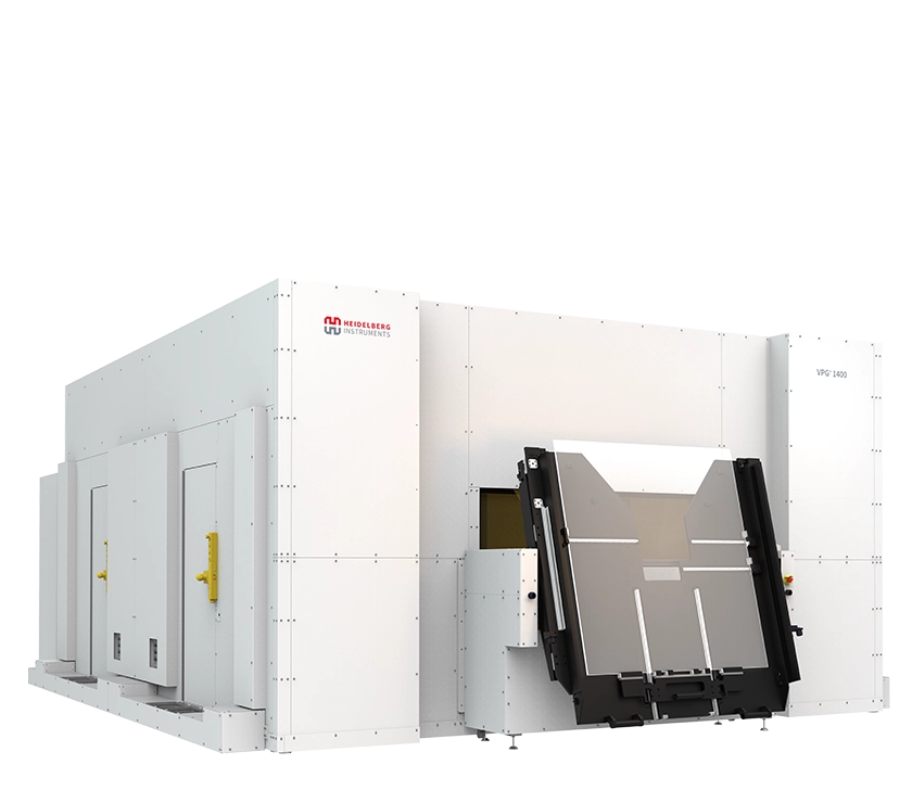
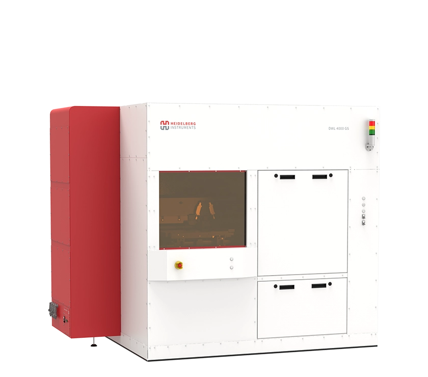
Heidelberg Instruments tools are utilized in multiple stages of display production, including the precise and uniform patterning of large photomasks, up to 1400 x 1400 mm² (VPG+ 1400), used for insulating and conducting layers prior to integrating liquid crystals or organic compounds (in LCDs and OLEDs). They succeed in generating highly uniform color-filtering arrays. They also find application in the fabrication of backlight illumination panels, in 2.5D micro-structures like diffusers or micro-lens arrays (DWL 2000 GS / DWL 4000 GS), and in the packaging process for integration into electronic devices (MLA 300).
Requirements
Solutions
Displays represent a fundamental component in modern electronics, providing visual interfaces for a wide range of devices, from smartphones to large-scale flat-panel displays (FPD). Display technologies depend on materials with diverse electrical conductivity, like ITO. These materials are layered onto substrates, forming the basis for pixelated displays. Utilizing photolithography, intricate patterns are transferred into these materials using masks or direct writing techniques.
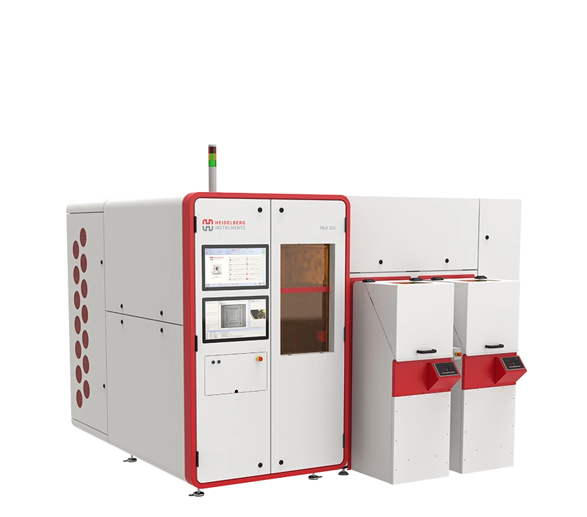
Heidelberg Instruments tools are utilized in multiple stages of display production, including the precise and uniform patterning of large photomasks, up to 1400 x 1400 mm² (VPG+ 1400), used for insulating and conducting layers prior to integrating liquid crystals or organic compounds (in LCDs and OLEDs). They succeed in generating highly uniform color-filtering arrays. They also find application in the fabrication of backlight illumination panels, in 2.5D micro-structures like diffusers or micro-lens arrays (DWL 2000 GS / DWL 4000 GS), and in the packaging process for integration into electronic devices (MLA 300).
Photomask production on large substrates, perfect for display applications.
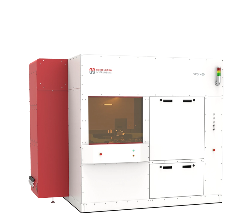
A production tool for standard photomasks and microstructures in i-line resists.
Maskless direct imager for high-accuracy and high-resolution microstructures.
A tool specifically designed to produce mature semiconductor photomasks.
The most advanced industrial grayscale lithography tool on the market.
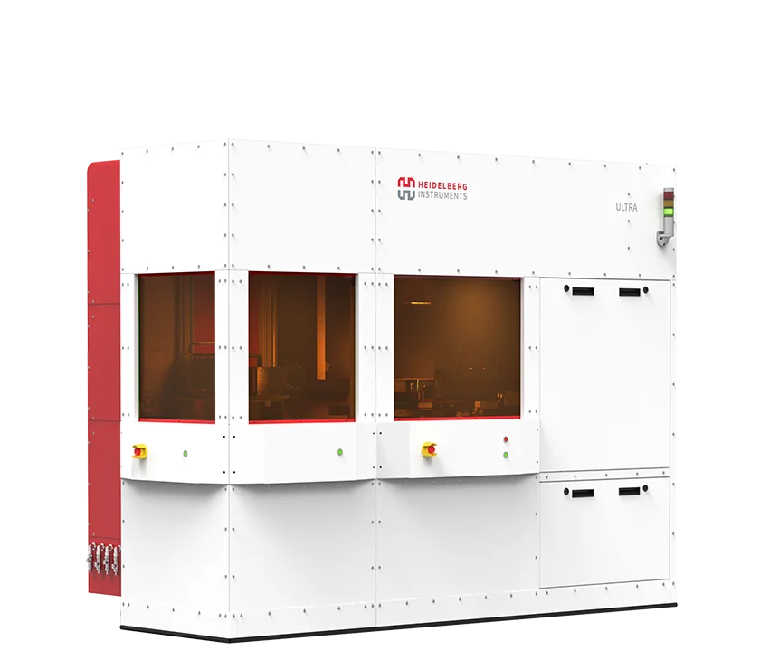
Optimized for industrial production with highest throughput and seamless integration into industrial production lines.
We are always at your disposal.
Please send us your request.
To view the form, please enable Marketing cookies.
Subscribe to our newsletter
to receive the newest information.
To view the form, please enable Marketing cookies.