There is a remarkable and rapidly growing interest in research and development activities focused on quantum devices worldwide. The potential of these future quantum devices to revolutionize computing, sensing, and data communication is tremendous. The prototypes and concepts for quantum devices are incredibly diverse, relying on a wide range of particles and quasi-particles, each chosen for their unique properties and interactions.
To support the advancements in quantum research, Heidelberg Instruments offers a comprehensive portfolio of tools that can manufacture various structures crucial for different areas of quantum research. Our extensive toolset includes the NanoFrazor systems, renowned for their ultra-high resolution capabilities. These systems allow for precise fabrication, minimizing damage and providing a bridge to future production. Additionally, our DWL series enables the creation of 2.5D topographies, while the VPG+ produces high-precision masks suitable for mass manufacturing. The MPO 100 tool is designed for manufacturing 3D micro-structures, and our Maskless Aligners (MLA) are ideal for multi-layer device fabrication.
In particular, the direct write lithography capabilities combined with high resolution offered by Heidelberg Instruments’ tools facilitate the development and production of quantum devices. Notably, the NanoFrazor stands out with its markerless overlay feature, leveraging the integrated reader for accurate alignment of multiple active regions on top of each other.
With Heidelberg Instruments’ portfolio of tools, researchers and engineers in the quantum field have access to advanced fabrication capabilities that enable them to push the boundaries of quantum device development. These tools support the realization of diverse quantum device concepts, paving the way for future breakthroughs in quantum computing, sensing, and data communication.
Required for well-defined features and gaps with low edge roughness
Damage-free nanolithography (NanoFrazor)
Non-destructive technique without using high-energy charged beams allows working with sensitive materials
Accurate overlay
Possible by simply drawing the electrodes onto the topography or optical image (NanoFrazor & MLA series)
Accurate grayscale lithography
Used for control of grayscale topographies down to the single nanometer
3D micro printing of optical interconnects
Used for high bandwidth data transmission and low power consumption (MPO 100)
There is a remarkable and rapidly growing interest in research and development activities focused on quantum devices worldwide. The potential of these future quantum devices to revolutionize computing, sensing, and data communication is tremendous. The prototypes and concepts for quantum devices are incredibly diverse, relying on a wide range of particles and quasi-particles, each chosen for their unique properties and interactions.
To support the advancements in quantum research, Heidelberg Instruments offers a comprehensive portfolio of tools that can manufacture various structures crucial for different areas of quantum research. Our extensive toolset includes the NanoFrazor systems, renowned for their ultra-high resolution capabilities. These systems allow for precise fabrication, minimizing damage and providing a bridge to future production. Additionally, our DWL series enables the creation of 2.5D topographies, while the VPG+ produces high-precision masks suitable for mass manufacturing. The MPO 100 tool is designed for manufacturing 3D micro-structures, and our Maskless Aligners (MLA) are ideal for multi-layer device fabrication.
In particular, the direct write lithography capabilities combined with high resolution offered by Heidelberg Instruments’ tools facilitate the development and production of quantum devices. Notably, the NanoFrazor stands out with its markerless overlay feature, leveraging the integrated reader for accurate alignment of multiple active regions on top of each other.
With Heidelberg Instruments’ portfolio of tools, researchers and engineers in the quantum field have access to advanced fabrication capabilities that enable them to push the boundaries of quantum device development. These tools support the realization of diverse quantum device concepts, paving the way for future breakthroughs in quantum computing, sensing, and data communication.
Ultra-high resolution patterning for well-defined structures (e.g., for tunneling gaps or plasmonic cavities)
Damage-free lithography, without deleterious effects on quantum materials (e.g., topological insulators)
Fast and accurate placement of electrodes on low-dimensional materials with unknown positions (2D material flakes, dispersed nanowires, etc.)
The grayscale environment and topography can be crucial for fine-tuning photon interactions in quantum devices
Rapid prototyping is a significant advantage in a dynamic research field.
Ultra-high resolution
Required for well-defined features and gaps with low edge roughness
Damage-free nanolithography (NanoFrazor)
Non-destructive technique without using high-energy charged beams allows working with sensitive materials
Accurate overlay
Possible by simply drawing the electrodes onto the topography or optical image (NanoFrazor & MLA series)
Accurate grayscale lithography
Used for control of grayscale topographies down to the single nanometer
3D micro printing of optical interconnects
Used for high bandwidth data transmission and low power consumption (MPO 100)
Application images
Waveguide 2 µm wide patterned with a DWL 66+ (WM HiRes @ 405 nm) in a positive resist AZ 1512 HS.
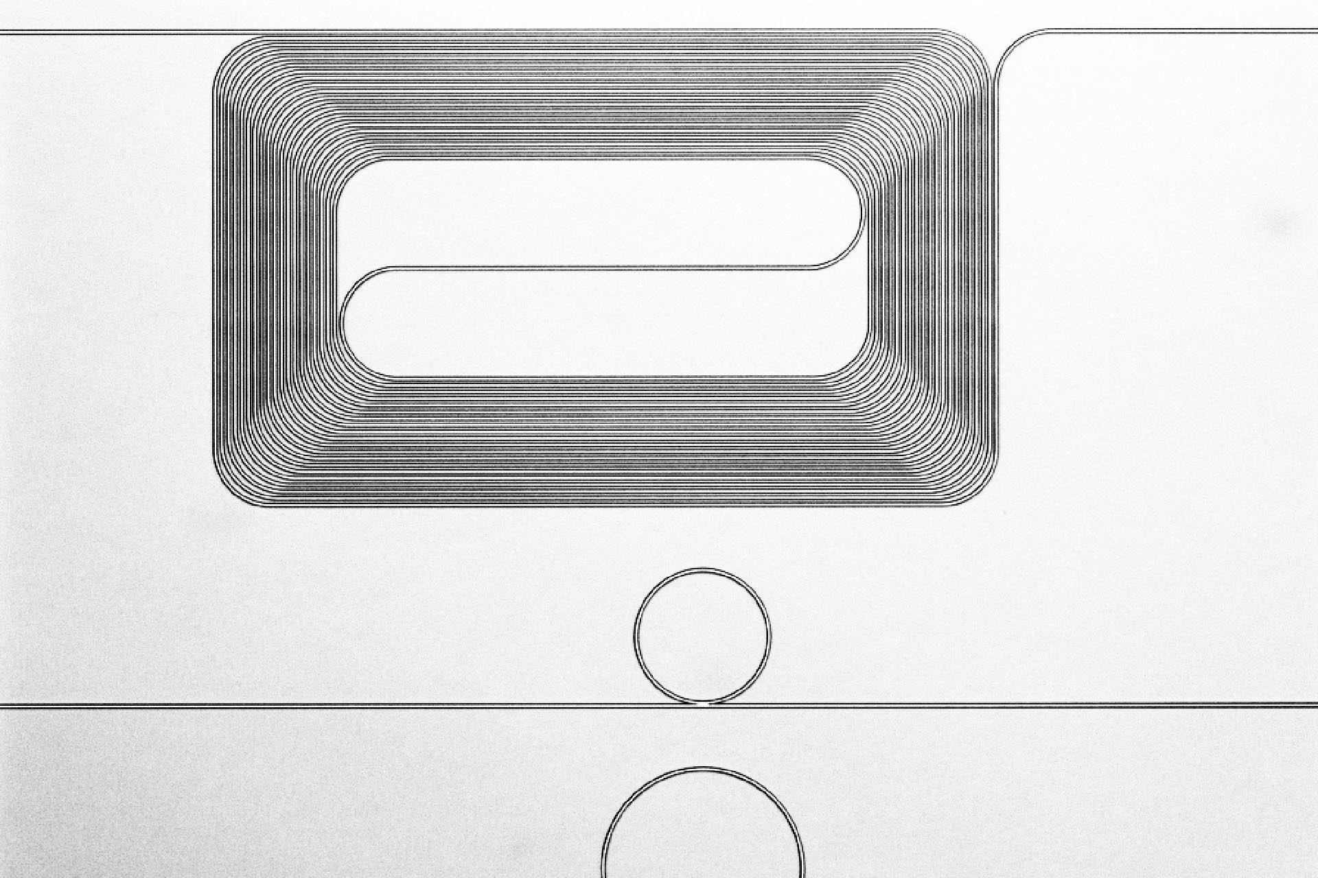
Results obtained on a DWL 66+ laser lithography system. The image shows 2 µm lines and circles in a 1.5 µm thick positive resist. The distance between the lines and circles is 500 nm.
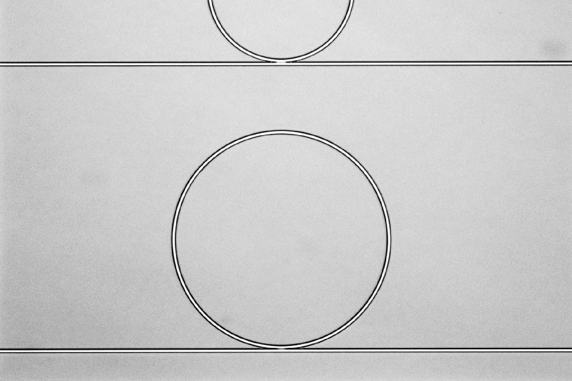
Rings exposed with a MLA 150 (WM I @ 375 nm) in a negative resist ma-N1405, diameter: 12 µm, width: 800 nm, thickness: 800 nm
Exposure showing 2 µm lines on a DWL 66+ laser lithography system. The distance between the lines
and circles is 500 nm.
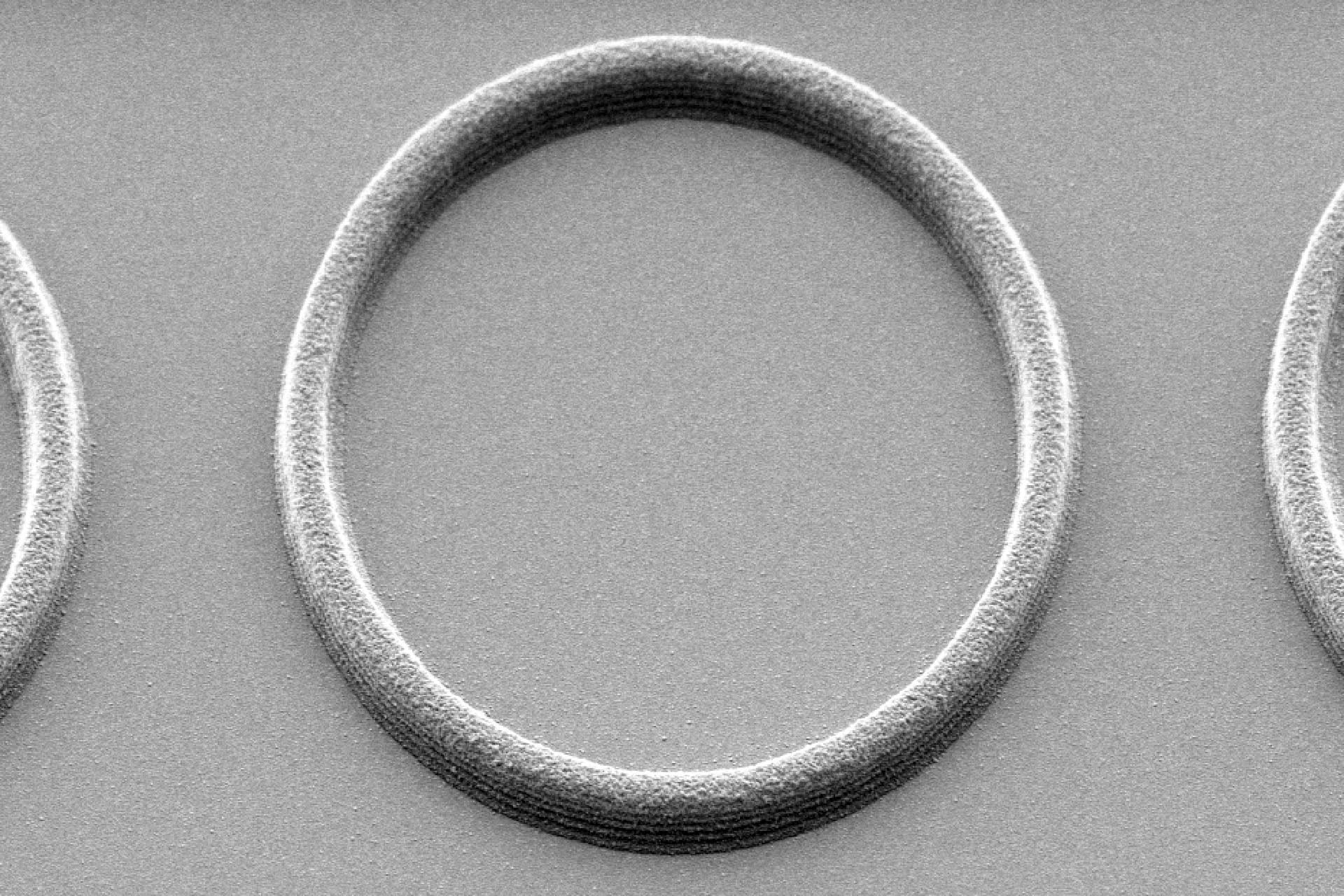
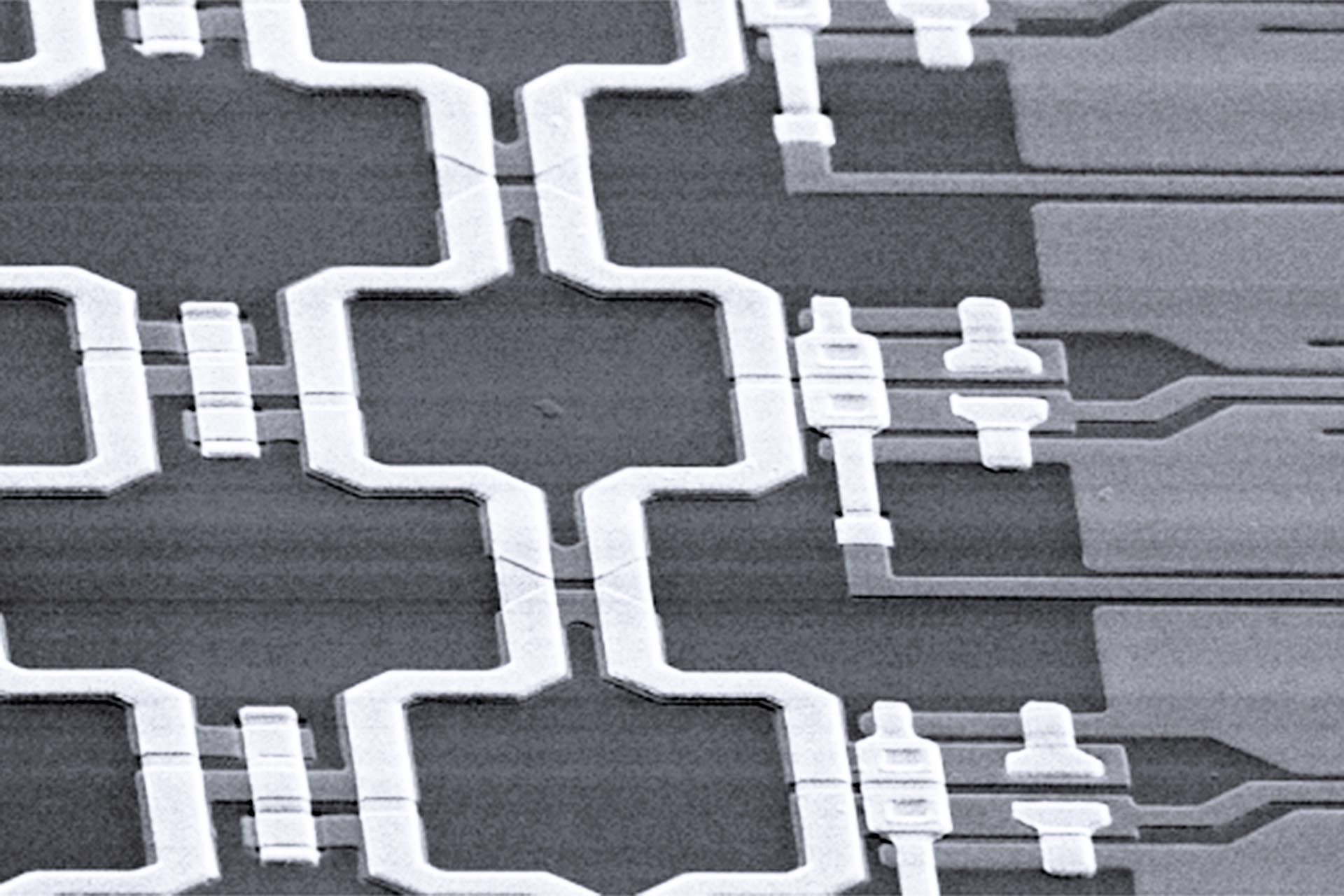
MLA 150: An array of SQUIDs (superconducting quantum interference device) used for the readout of metallic magnetic microcalorimeters (high-resolution particle detectors operated at low temperatures).
(Courtesy of the Kirchhoff Institute for Physics (KIP), Heidelberg University)
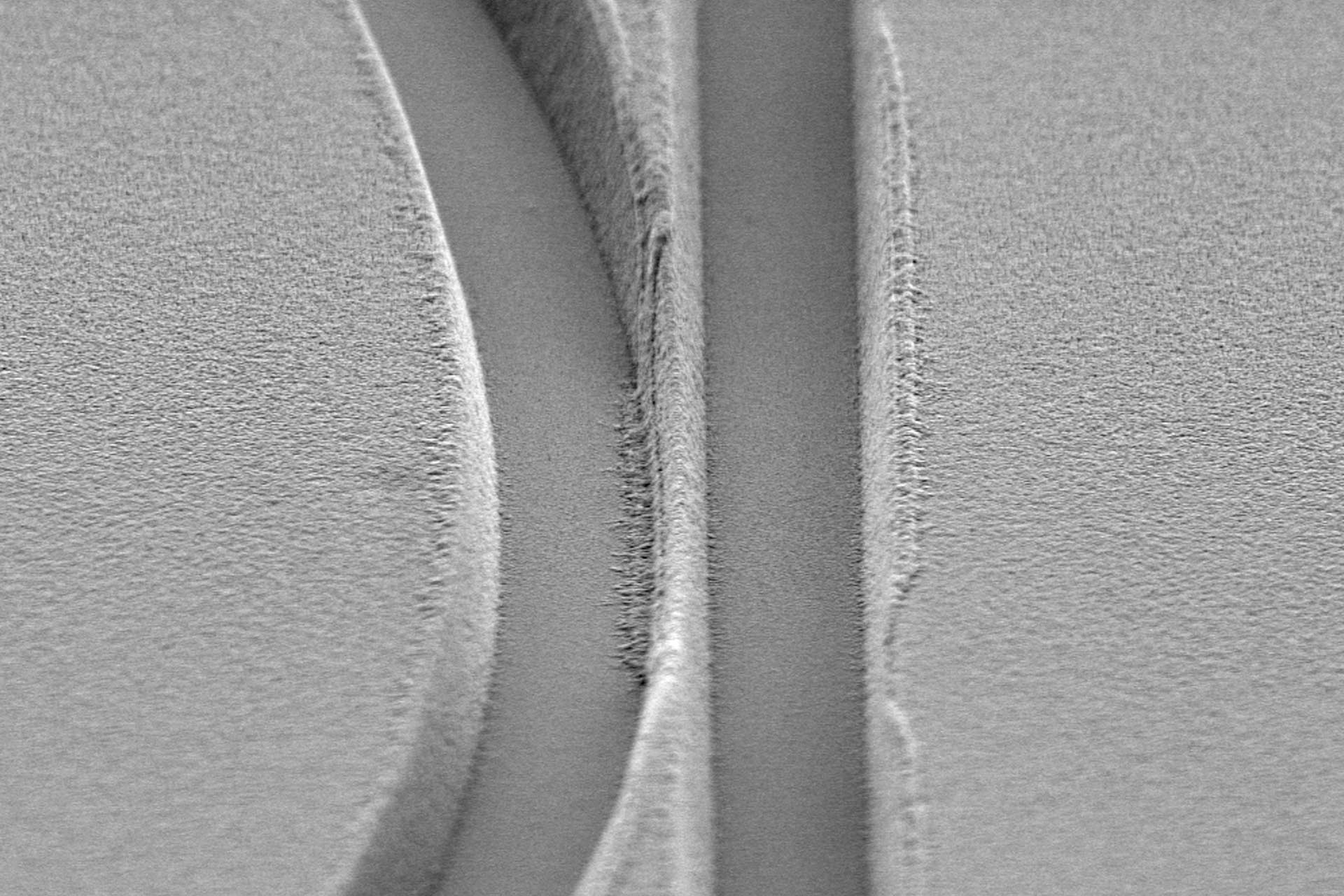
Sharp vertical Ag electrodes made with the NanoFrazor tip.
(Courtesy of Prof. Leuthold group, ETH Zurich, Publication in 2019)
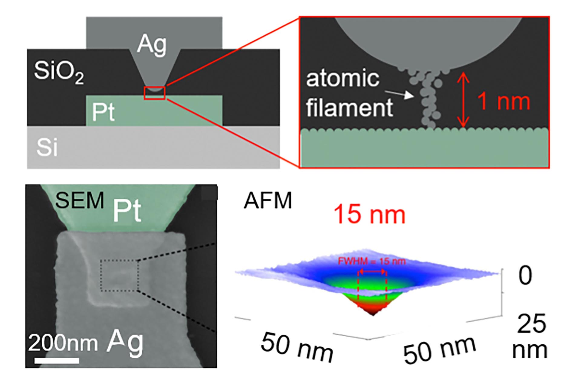
AFM image of an MBE-grown Ge nanoribbon (blue line in the inset) with top gates patterned by NanoFrazor. The device is fabricated in order to study the topological states in the ribbon.
(Courtesy of Prof. Georgios Katsaros, IST Austria and Heidelberg Instruments Nano)
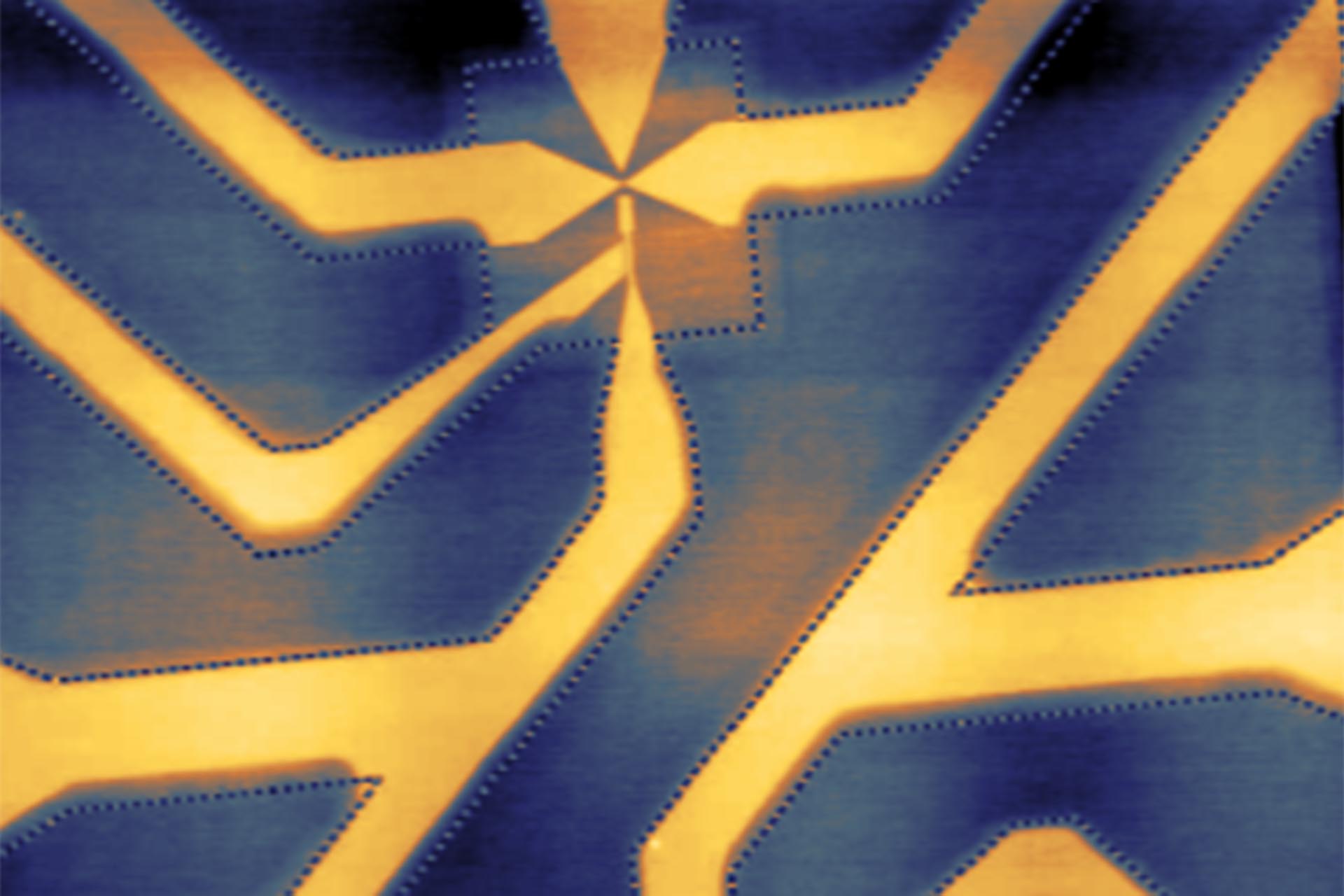
NanoFrazor: Silicon quantum dot single electron transistors
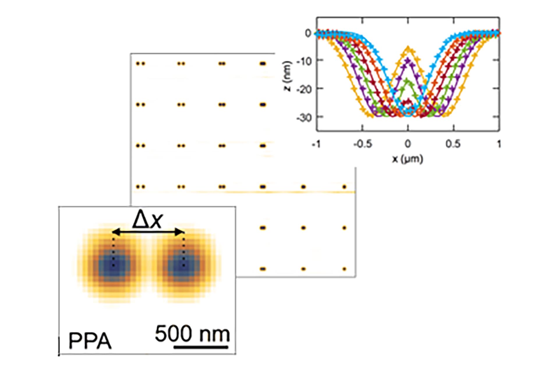
Gaussians with varying distance ∆x fabricated using PPA lithography and transferred onto a SiO2 substrate, to be stacked in a distributed Bragg reflector, forming a photonic molecule structure. A precise Gaussian profile is patterned using the NanoFrazor and the closed-loop lithography approach. (Courtesy of IBM Research Zurich, publication in 2018)
suitable Systems
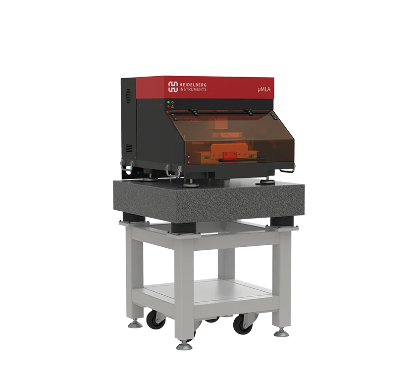
µMLA
Maskless Aligner
Configurable and compact tabletop maskless aligner with raster scan and vector exposure modules.
DWL 66+
Direct Write Laser Lithography System
Our most versatile system for research and prototyping with variable resolution and wide selection of options.
DWL 2000 GS / DWL 4000 GS
Direct Write Laser Lithography System
The most advanced industrial grayscale lithography tool on the market.
MLA 150
Maskless Aligner
The fastest maskless tool for rapid prototyping, the alternative to the mask aligners. Perfect for standard binary lithography.
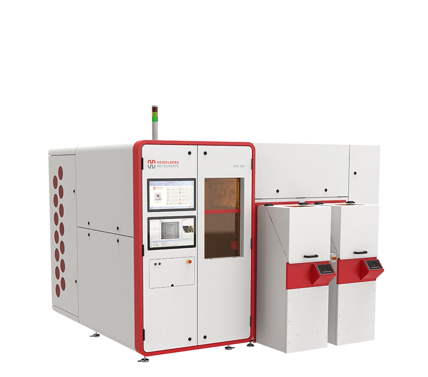
MLA 300
Maskless Aligner
Optimized for industrial production with highest throughput and seamless integration into industrial production lines.
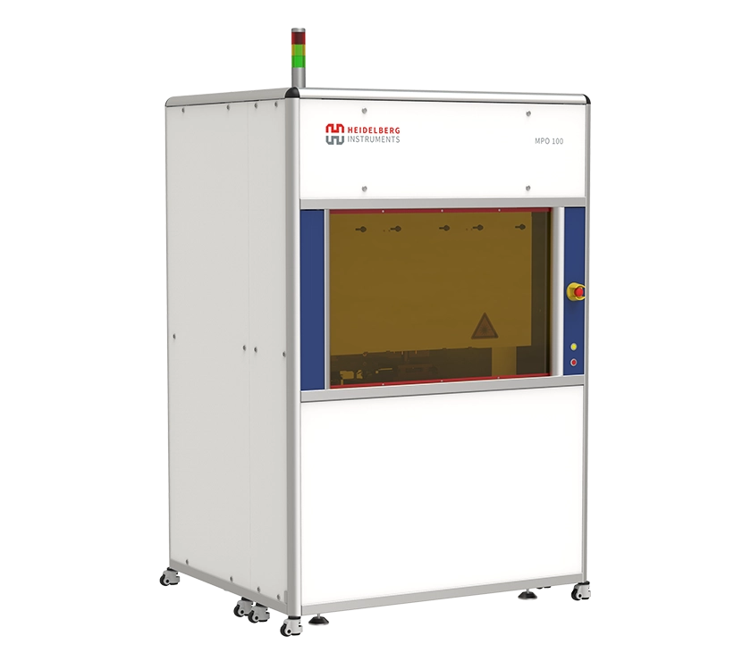
MPO 100
Two-Photon Polymerization Multi-User Tool
Multi-User Tool for 3D Lithography and 3D Microprinting of microstructures with applications in micro-optics, photonics, micro-mechanics and biomedical engineering.
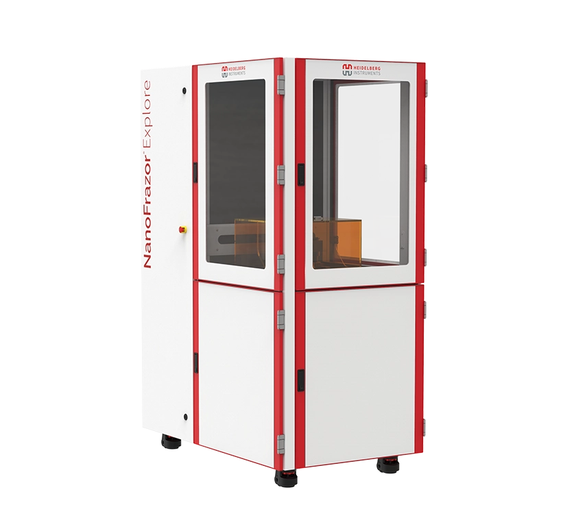
NanoFrazor Explore
Thermal Scanning Probe Lithography System
Thermal scanning probe lithography tool with direct laser sublimation and grayscale modules. Excellent alternative to e-beam lithography tools.