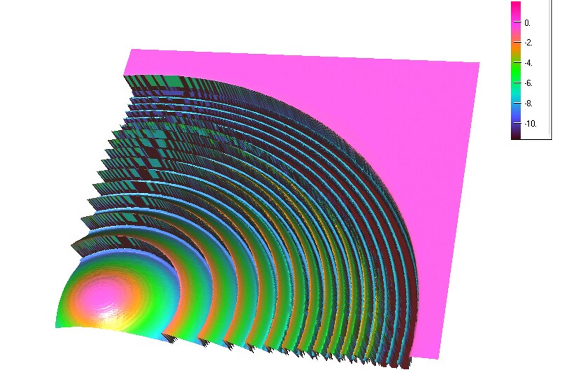
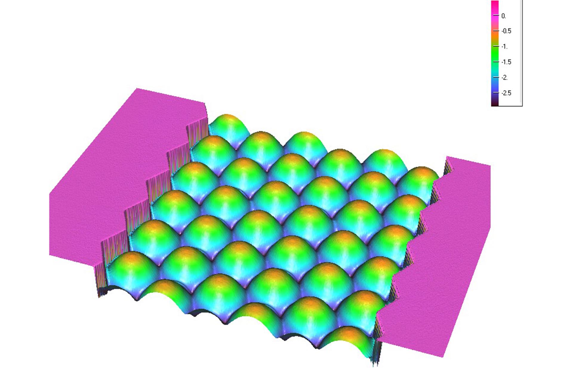
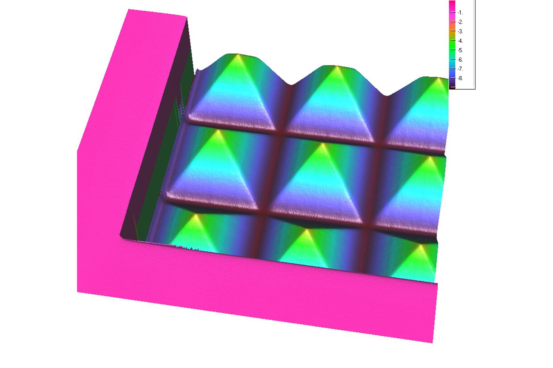
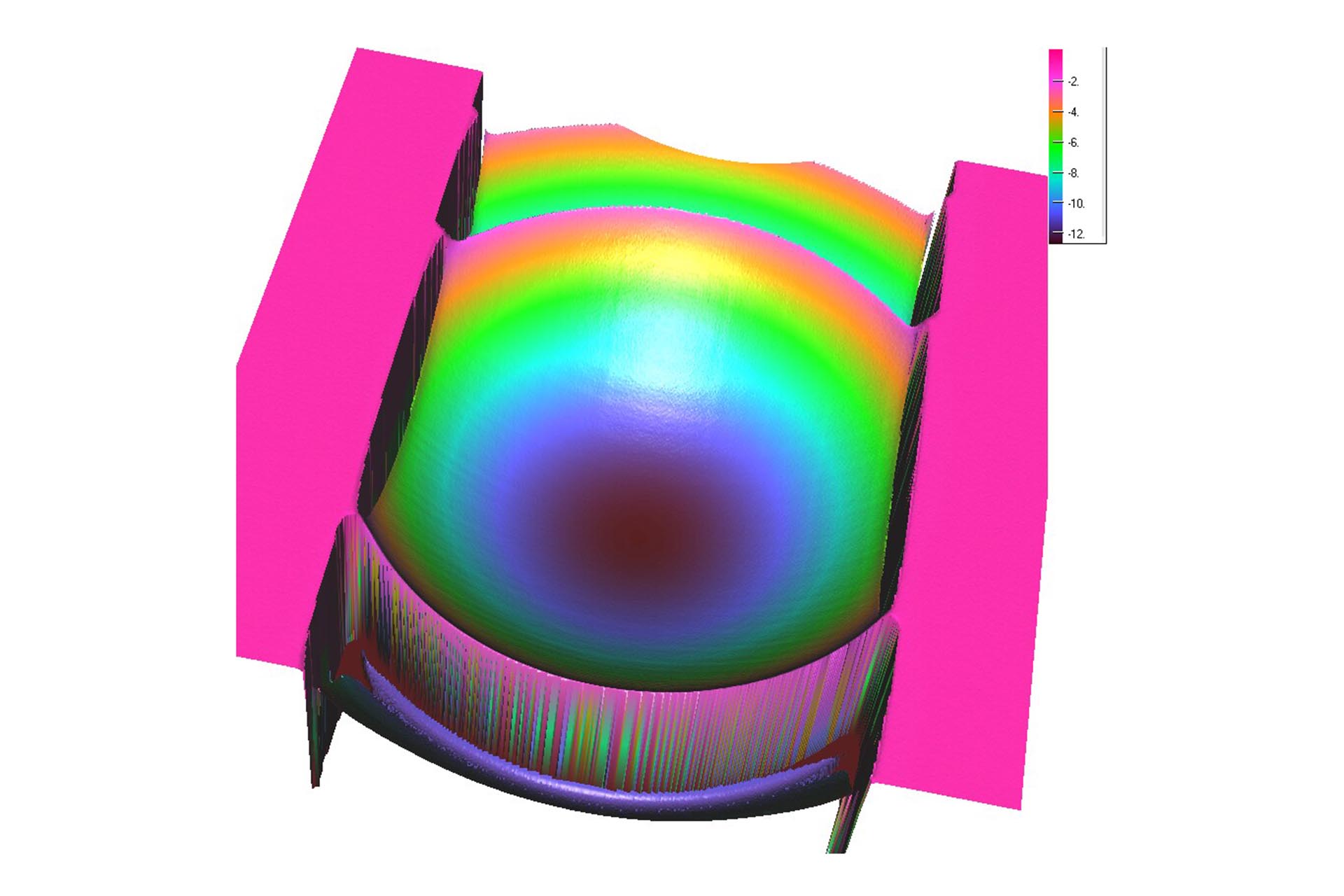
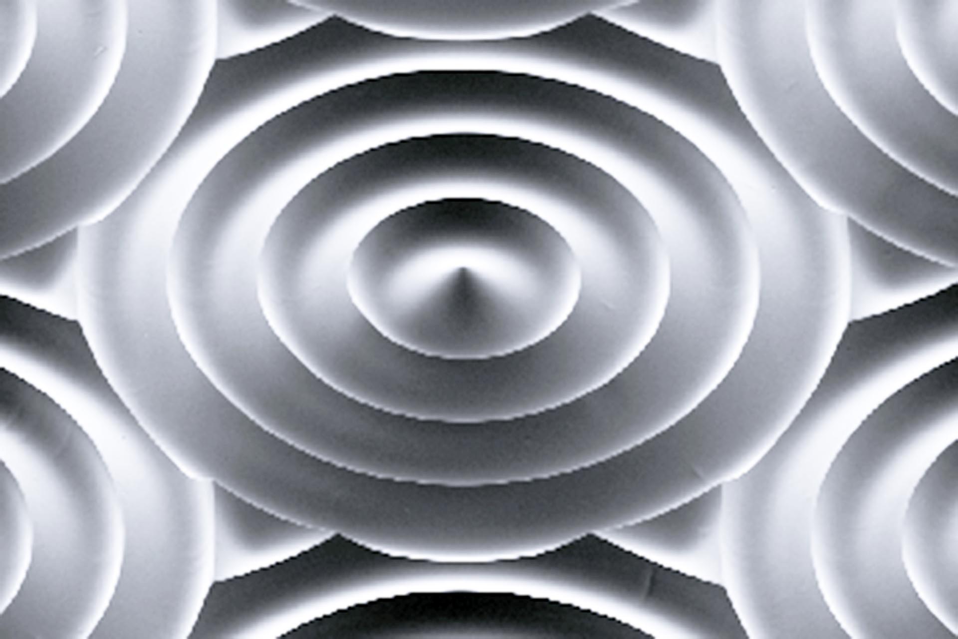
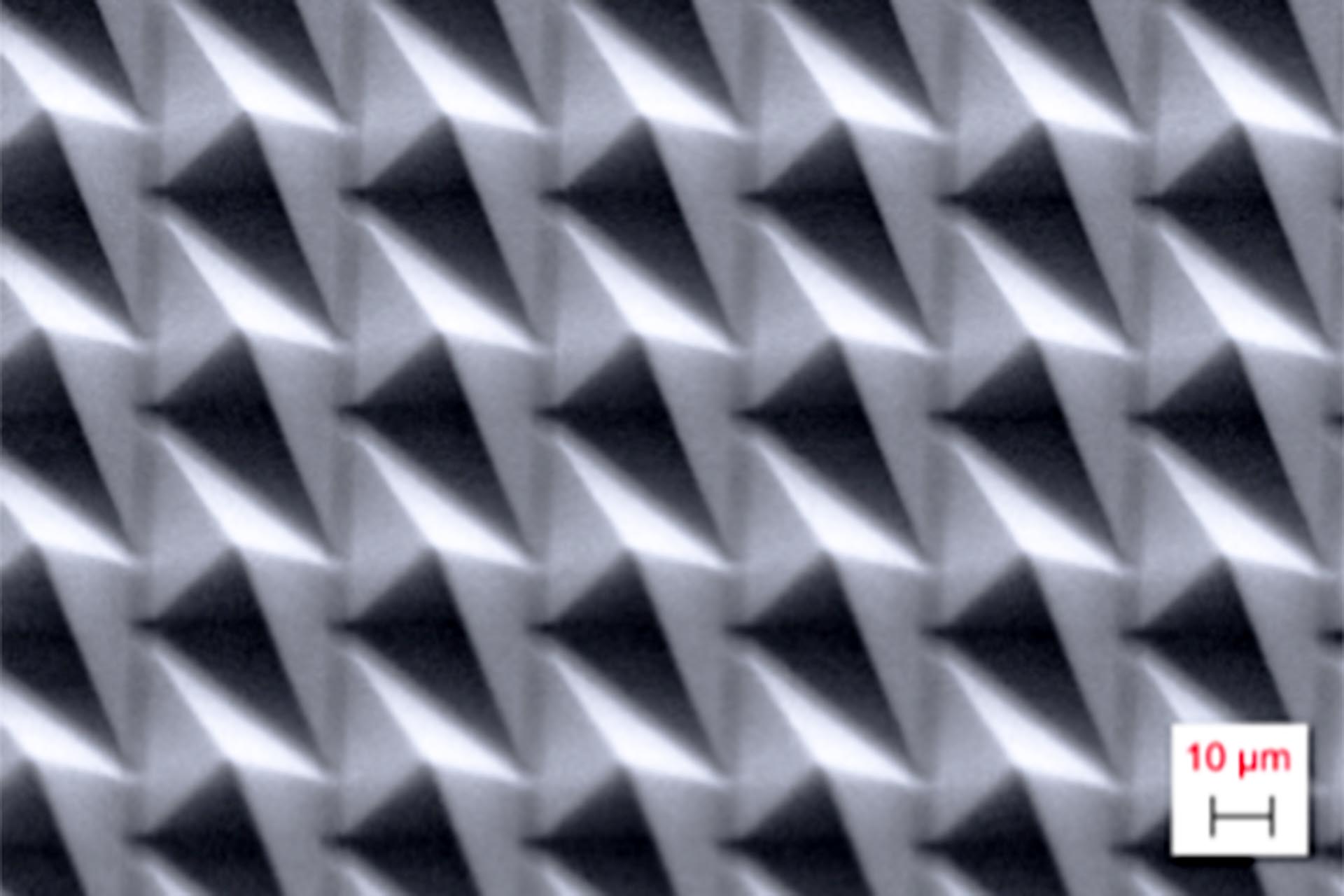
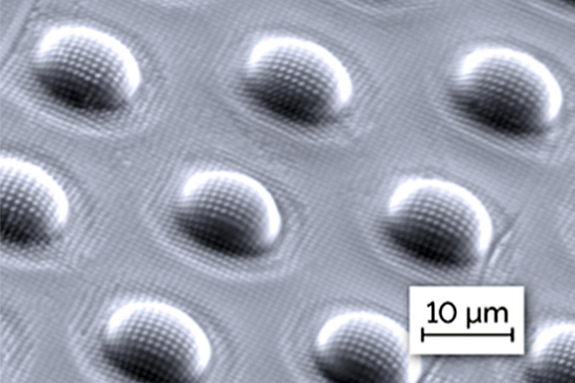
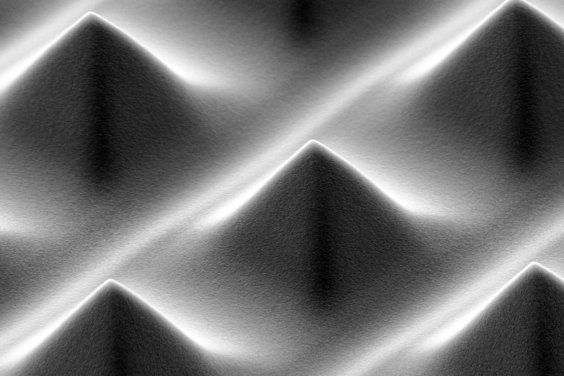
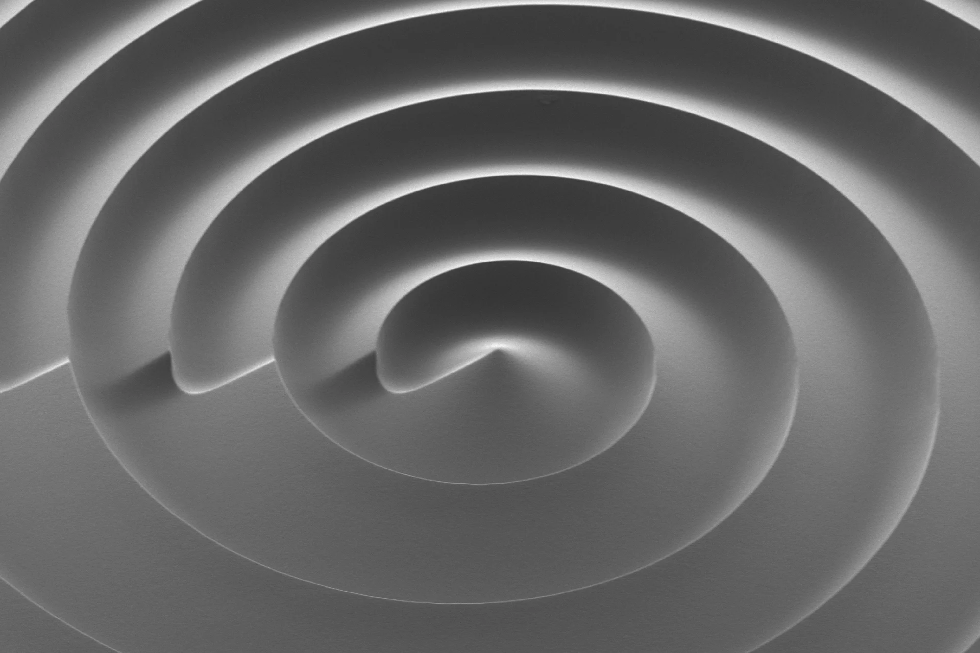
Heidelberg Instruments’ systems use Grayscale lithography for the creation of 2.5D micro- and nanostructures with varying height gradients, enabling the fabrication of surfaces with complex topographies.
In direct write laser lithography, the CAD virtual landscape is mapped to the system’s gray values where each value corresponds to an exposure intensity level. During the exposure, the system modulates the laser intensity on a pixel-by-pixel level, thereby controlling the exposure depth for each individual pixel. Up to 1024 gray levels are accessible in a single exposure step, offering the highest vertical resolution without critical alignments. The resulting exposure is then processed by methods such as RIE or electroplating to create the 2.5D topography. The grayscale exposure concept is also scalable, with systems capable of patterning substrates up to 800 mm x 800 mm in size. Common challenging issues, such as stitching effects and non-linearities, are solved with advanced patterning techniques such as multi-pass exposures and optimized gray value distributions.
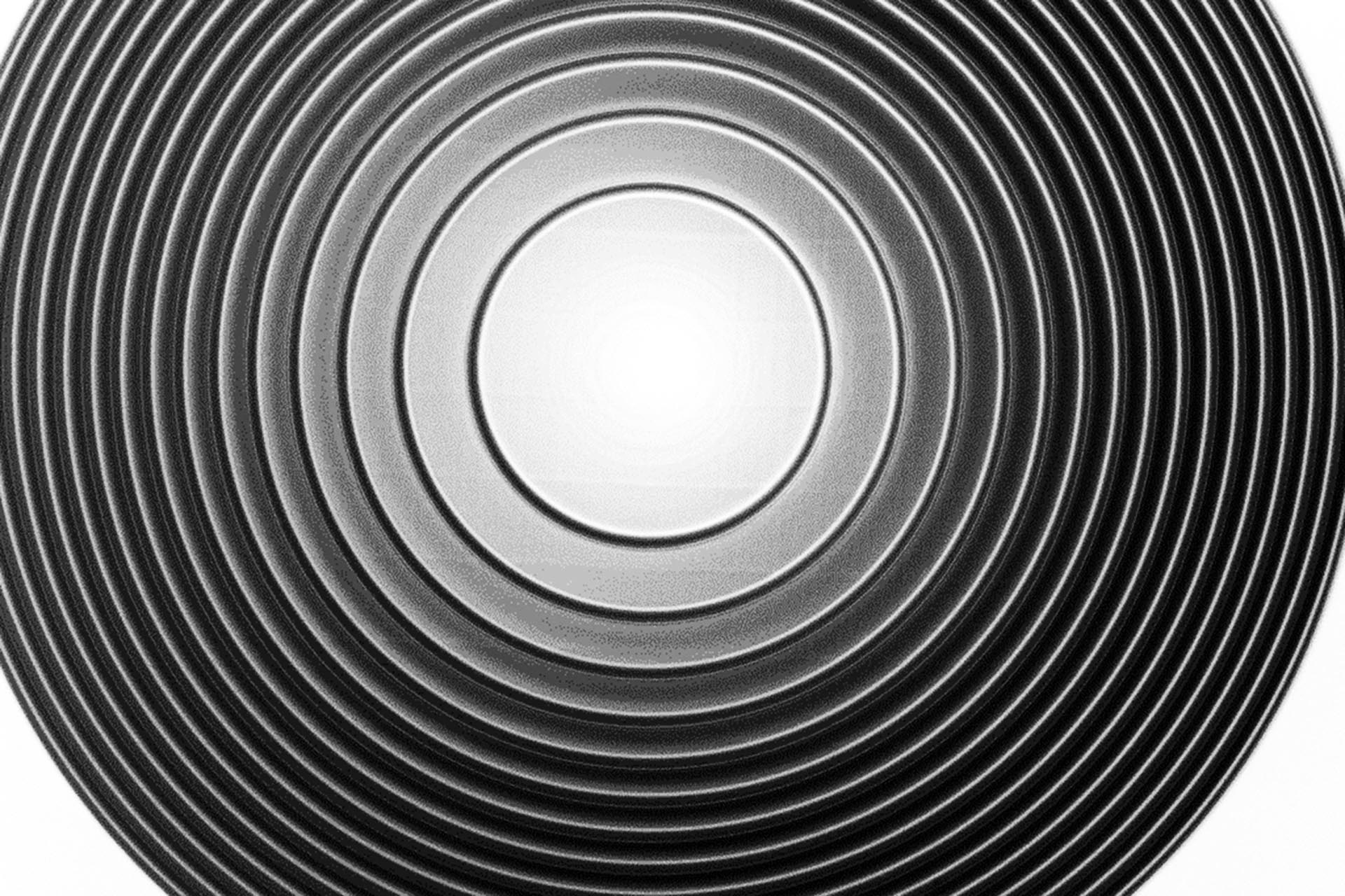
A key application area for grayscale lithography is the creation of micro-optical elements such as Fresnel lenses, blazed gratings, micro-lenses, and micro-lens arrays, all of which are key components in modern day micro-optics. Grayscale lithography can also be used in the creation of MEMS, MOEMS, microfluidic devices, and textured surfaces.
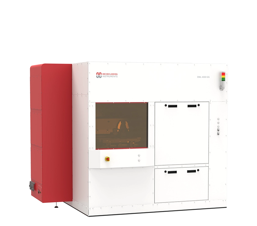
Heidelberg Instruments offers numerous grayscale packages, depending on the required performance level for the application.
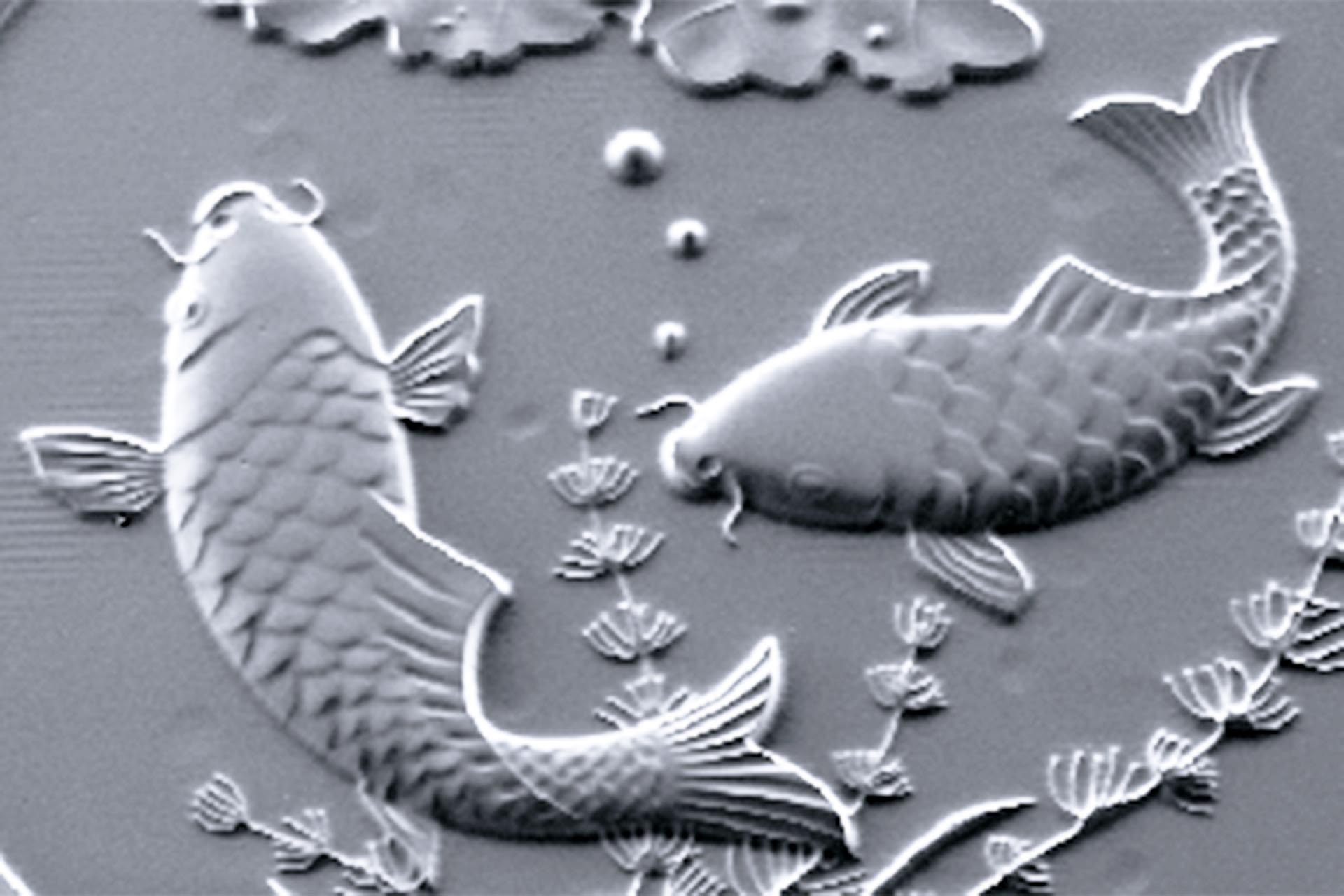
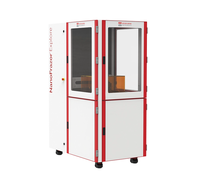
Our NanoFrazor systems enable grayscale patterning using thermal scanning probe lithography. Specifically, the NanoFrazor Explore and NanoFrazor Scholar use an ultra-sharp heated silicon tip to pattern high resolution 2D and 2.5D structures by sublimating a thermally sensitive resist. The structures can then be transferred into almost any other material by standard methods. This technique of lithography requires no wet development and causes no damage to the substrate. Lateral resolutions of below 25 nm are routinely achieved with these systems. Additionally, the closed-loop lithography method enables a vertical resolution of less than 1 nm. Application areas for the NanoFrazor systems include CGH’s, 3D multimode waveguides, and grating couplers, 3D phase plates, and many other areas that require 2.5D nanostructured surfaces.