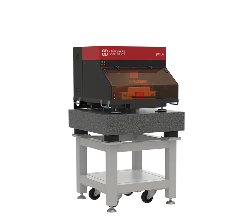
Many applications require lithography on special samples other than the standard wafer and mask formats. We have gathered a lot of experience with unique requirements for different substrates. In research, small pieces of wafers are commonly used. Therefore, our complete R&D product portfolio is specialized to work easily on samples as small as a few millimeters.
Other applications require lithography on unconventional substrates such as long rods, prisms, or even curved surfaces. If your application requires unusual substrates, talk to us.
Most of our standard systems can already handle a wide variety of substrates, and we can develop custom systems for almost any size and type of substrate. Heidelberg Instruments manufactures the stages in-house at our headquarters in Heidelberg.