Direct Write Optical Waveguide Fabrication in organic films using a Heidelberg Laser Writer
Cheap and quick fabrication of mr-DWL waveguides channels on glass buried in optical polymer cladding with 350 µm radius ring resonators and 0.9 µm spacing.
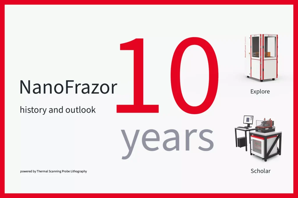
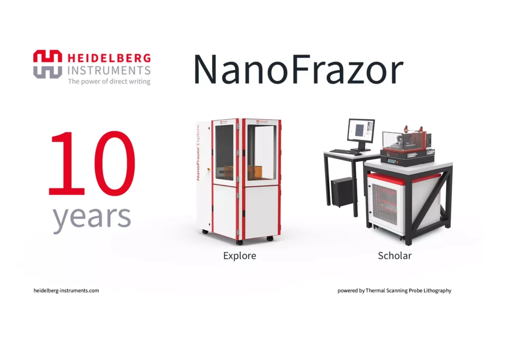
The commercialization of the NanoFrazor started in 2012. This article looks back at where the NanoFrazor came from, how it
Zurich, Switzerland / Heidelberg, Germany – Heidelberg Instruments Nano AG in Zurich, a subsidiary office of Heidelberg Instruments Mikrotechnik GmbH

Würzburg, Germany / Brisbane, Australia – The Australian National Fabrication Facility – Queensland Node (ANFF-Qld) based at the University of

Join our expert Dr. Jana Chaaban in this webinar to discover more about the working principle of the NanoFrazor lithography.

Heidelberg Instruments at the LASER World of PHOTONICS is all about the Power of Direct Writing After almost three years,
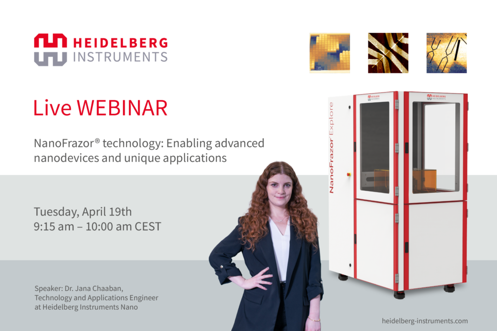
NanoFrazor technology: Enabling advanced nanodevices and unique applications register now The NanoFrazor uses thermal scanning probe lithography (t-SPL) for the

Heidelberg, March 30, 2022. Heidelberg Instruments has received a significant order from a leading semiconductor wafer-level packaging production company in
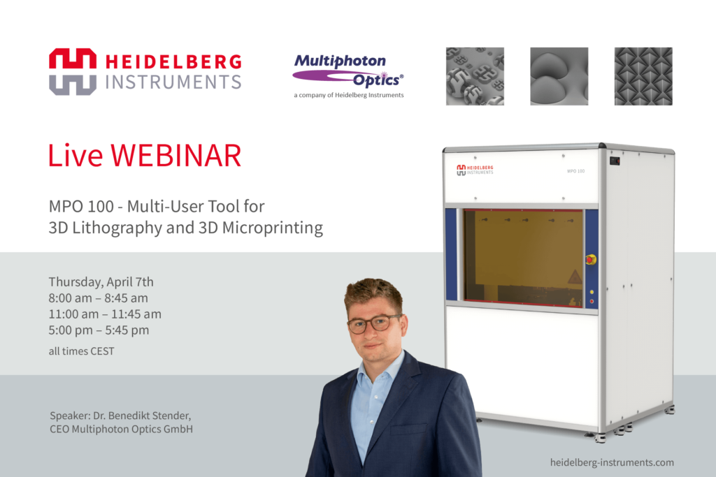
MPO 100 – Multi-User Tool for 3D Lithography and 3D Microprinting „1 – 10 – 100 – 1000” – Achievable
EPIC Virtual Company Tour at Heidelberg Instruments and Multiphoton Optics The European Photonics Industry Consortium (EPIC), Multiphoton Optics and Heidelberg

The SPIE Photonics West, the leading global conference in San Francisco, brings together experts in industrial lasers, optoelectronics, biomedical, optics