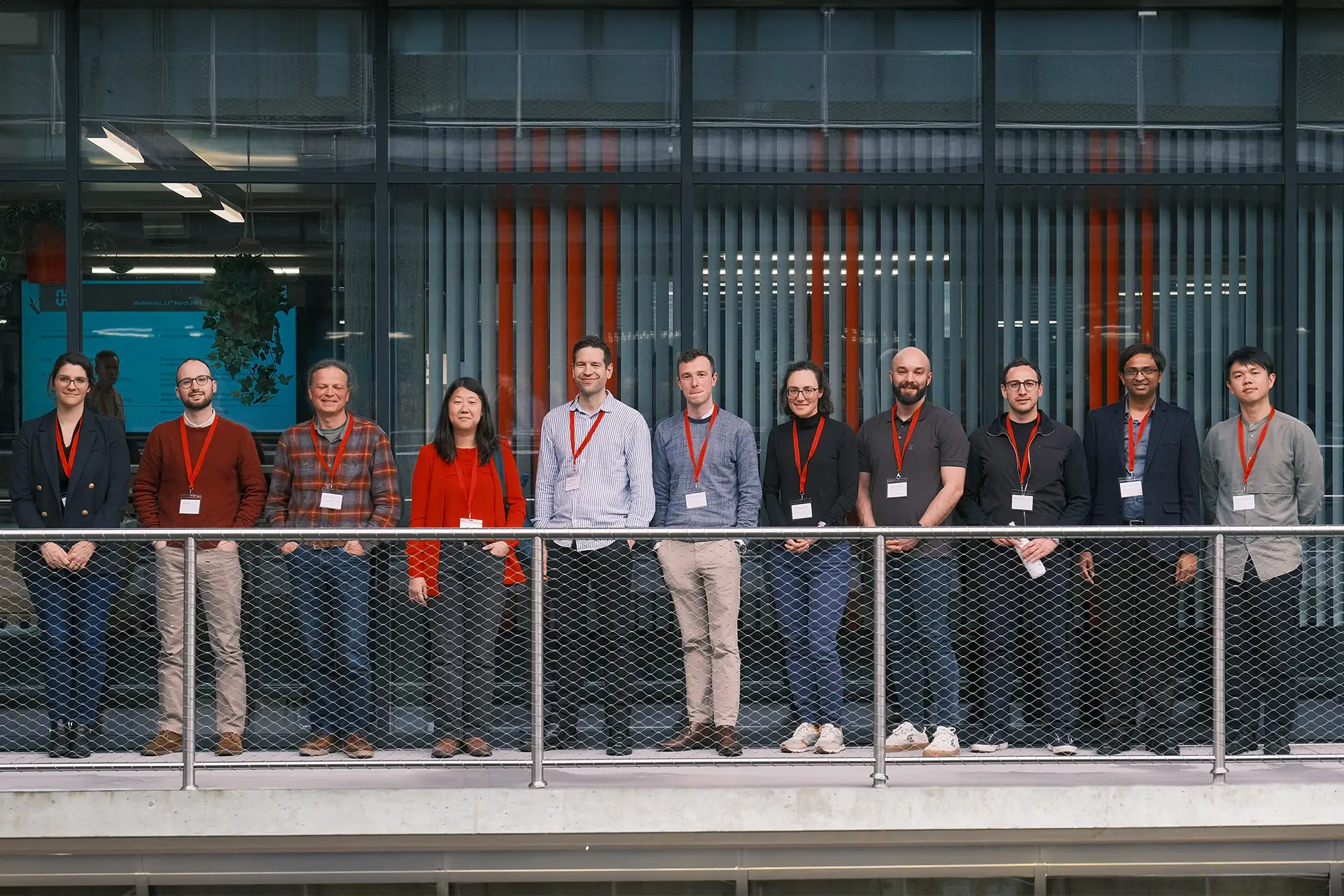
EPIC Virtual Company Tour at Heidelberg Instruments and Multiphoton Optics
The European Photonics Industry Consortium (EPIC), Multiphoton Optics and Heidelberg Instruments invite you to join us Tuesday, March 22nd from 4:00 pm – 5:00 pm (CEST) on Zoom for a live guided company tour.
Step inside our state-of-the-art facilities to meet our team and learn more about our maskless lithography, thermal scanning probe and two-photon polymerization technologies.
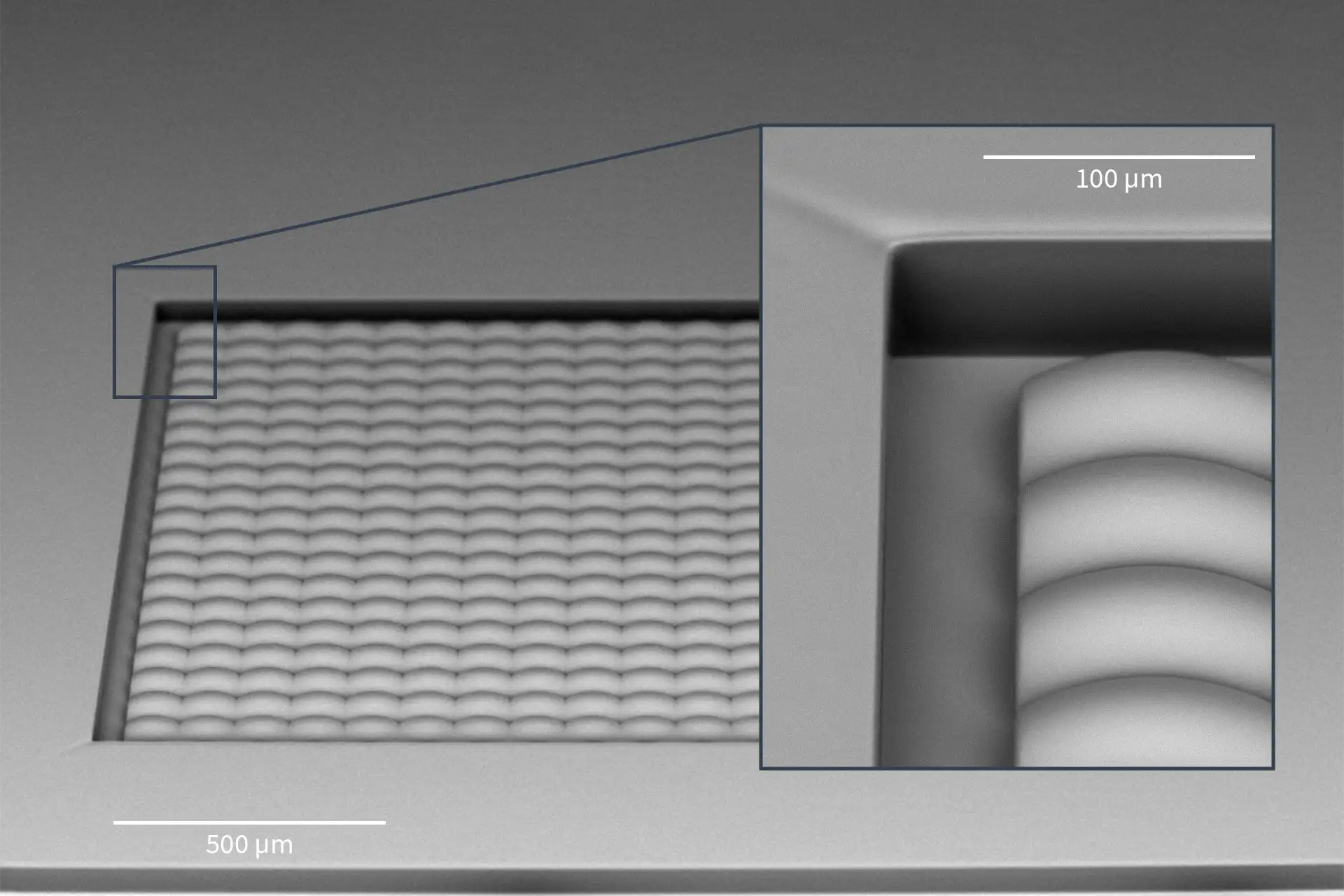
The virtual event will beginn with a tour at our new headquarter in Heidelberg, Germany and will give you the opportunity to get acquainted with our maskless lithography systems. The tour is designed to provide you with an understanding of how our facility works – showing you the production and assembly of our systems, the Process and Application Lab (PAL) for system performance benchmarks while taking you through the the grayscale lithography process.
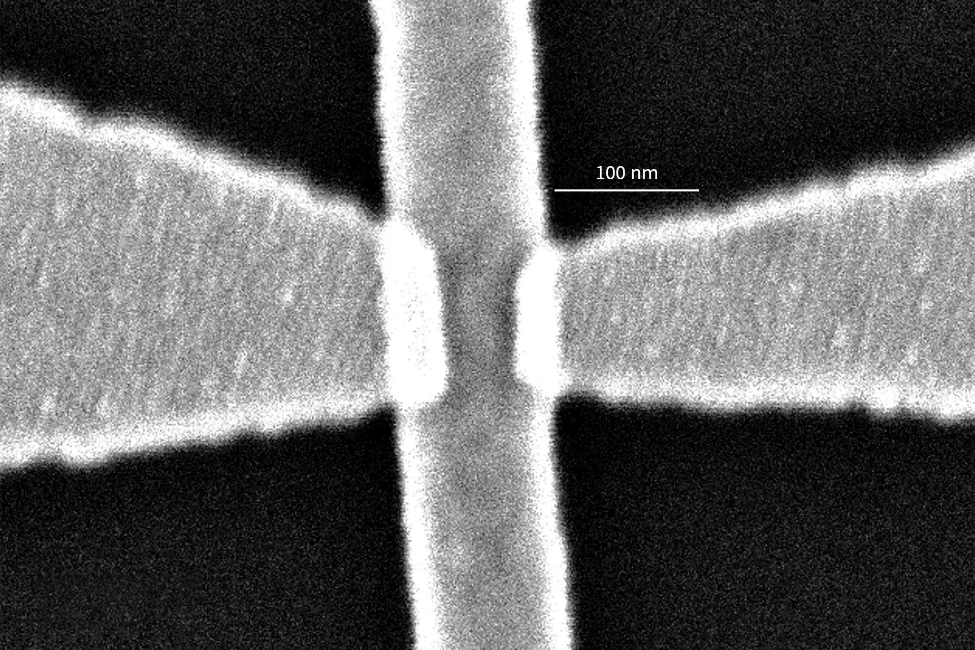
Directly after this, we will switch locations and stop by our colleagues at Heidelberg Instruments Nano in Zurich, Switzerland. Here you will receive more insights into our nanofabrication tools, the thermal scanning probe lithography (t-SPL) technology and the patterning process of the NanoFrazor systems.
Back in Germany, we will travel to our youngest Heidelberg Instruments family member, Multiphoton Optics, in Würzburg to learn more about their newly-launched MPO 100 Multi-User Tool for 3D Lithography and 3D Microprinting including the key features of this unique system, the core technology Two-Photon Polymerization (TPP) and how you can realize your design ideas.
Take this opportunity to sign up for this live virtual tour for a close-up look at our locations and see what makes us a world leader in the development and production of direct write lithography systems.
You can also follow the live event via YouTube stream.