Interview with Steffen Diez
Steffen Diez, the COO of Heidelberg Instruments, has seen the Maskless Aligners series from the initial idea conception to successful commercial release of 3 tools in the series: MLA150 optimized for R&D, a table-top version (μMLA) and the recently launched industrial machine MLA 300.
Steffen, thank you for finding the time to talk about the MLA series. Congratulations on the launch of MLA300 and your new role in the company (This interview was taken in 2019, recently after Steffen Diez was appointed COO – ed.). By the way, how did you begin at Heidelberg Instruments?
Steffen Diez: Thanks a lot. I started at Heidelberg Instruments in 2000 as a software engineer. We were only around 30 people at that time and the business was just starting to pick up. Over the years, I had the chance to look into almost every part of our company. I worked in Research and Development (R&D), led several projects, did benchmarking and customer demonstrations, and then switched to Technical Sales and Product Management. In 2012, after a one-year stay in Japan, I was invited to join the Technical Board, a group of experts managing all technical aspects of our company. This was when we decided to develop the first Maskless Aligner (MLA150). A few years later, in 2017, I joined the executive team of Heidelberg Instruments together with Martin Wijnaendts and Konrad Roessler. After a recent Heidelberg Instruments restructuring, I am now the Chief of Operations.
So, why a Maskless Aligner?
We actually hit upon this idea during a customer visit in a multi-user cleanroom which housed one of our DWL 66 systems (a powerful direct-write lithography tool). That DWL was used to produce masks for several mask aligners in the same cleanroom, some of them already quite old. We thought that replacing the Mask Aligner by a maskless tool for R&D applications could be a good opportunity for us. Even before we introduced the Maskless Aligner, direct writing was already a well-known technology in R&D. µPG 101 (our table-top direct writing tool) and the DWL 66 were installed in many facilities, but most of the time they were employed for producing photomasks instead of writing directly on wafers. And indeed, at that time our systems were optimized for photomask fabrication rather than for direct patterning of various substrates and photoresists. Even more critically, the exposure times were long as compared to a mask aligner. That was one of the biggest challenges we had to overcome with the MLA.
Tell us more about the development of the system. Which challenges did you face?
To develop the MLA technology, we used new MEMS-based optical modulators that just became available, and solid-state light sources to build new high-speed optical engines. This combination formed the core of the MLA and allowed us to significantly speed up the exposure. Apart from the exposure time, we also wanted to reduce the entire process runtime. Another important challenge we wanted to address is to improve usability and decrease user training time as much as possible: in facilities, where many users operate the tools, this is crucial. Taking all those requirements into account we set three main targets:
- Exposure time under 10 minutes for a 4″ wafer;
- Complete runtime including substrate loading and alignment under 30 minutes for a 4″ wafer;
- Training time of less than 1 hour to fully qualify as a user for system operation.
MLA owes its success to the clear vision of what we wanted to achieve and an outstanding, motivated development team. Based on the overall concept, the team implemented many ideas which transformed our vision into an exceptional tool, the MLA150.

What is so special about the MLA tools?
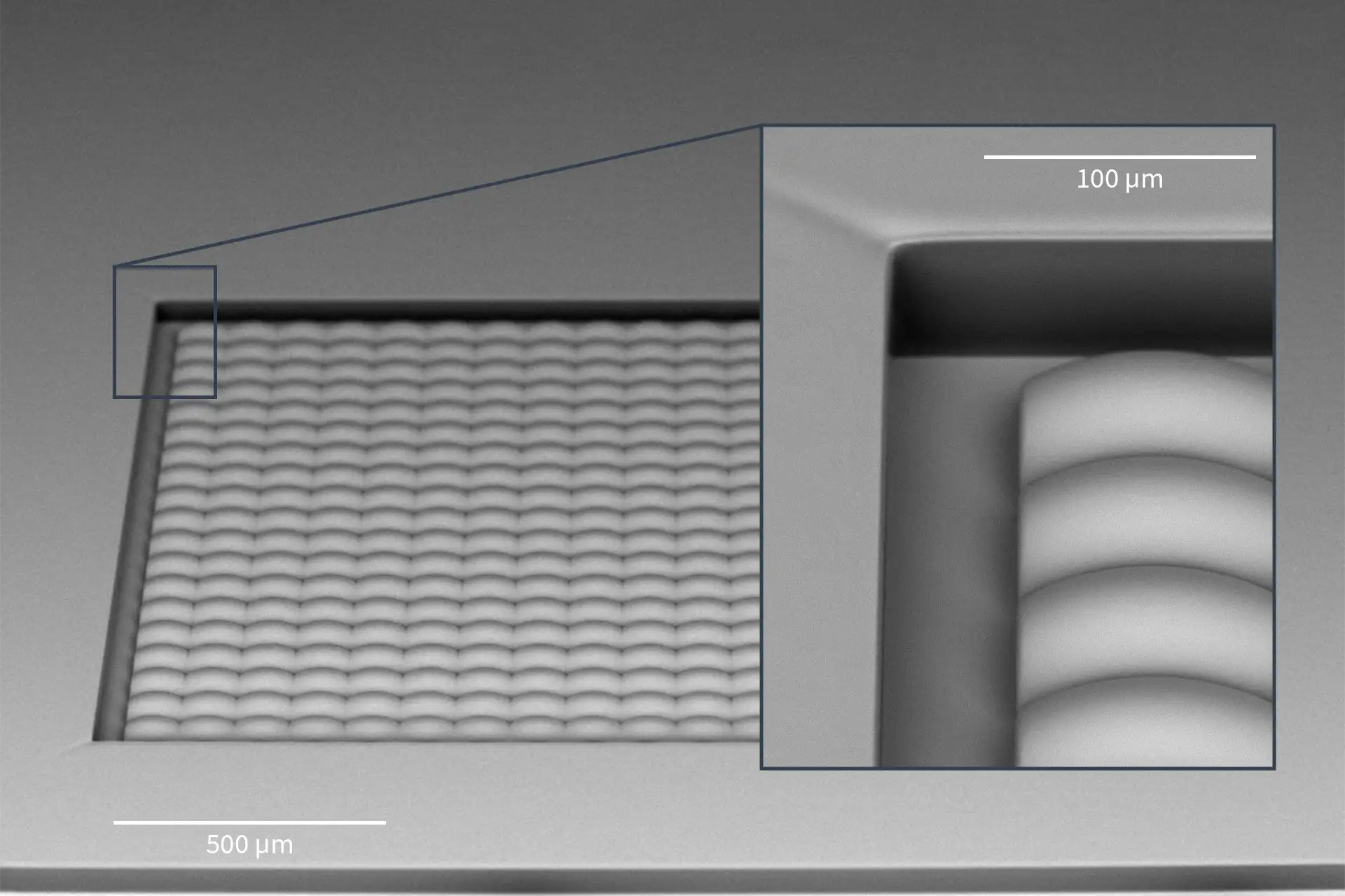
They were and still are the first and only tools which have become a real alternative for mask aligners in an R&D environment: They offer extremely high exposure speed; front- and backside-alignment; warpage compensation; high resolution and high accuracy; and the ability to expose on any substrate sizes from few-mm wafer pieces up to full 8″ wafers.
When did you introduce the first system? Did you collaborate with any potential users to develop and test the tool?
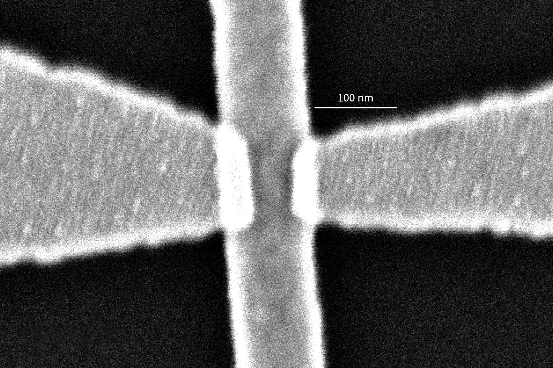
The MLA150 was officially introduced with a big marketing campaign in May 2015. After we developed the first working prototype, we decided to work together with a few selected users to evaluate and refine the tool. Main focus besides stability and bug-fixing was to optimize the usability of the system. The first beta-site was established at the CMi (Center for MicroNanoTechnology at EPFL in Lausanne). This facility was already our long-term customer and it has an outstanding reputation. Philippe Fluckiger, the head of CMi, did not hesitate to enter a collaboration after the concept of the MLA had been presented to him. The CMi team helped us a lot to optimize the user interface and eliminated most of the critical bugs. The second beta-site was in the group of Andreas Fleischmann and Sebastian Kempf from the Kirchhoff Institute of Physics in Heidelberg. They are world leaders in the research on SQUIDs, superconducting quantum interference devices that are used as low-temperature magnetic field sensors. Here, we focused on transferring multi-layer processes from their old mask aligner to our MLA. These applications have very demanding requirements for overlay accuracy, and we had to enhance the performance of our tool in many aspects even further to match the required specification. This was a very successful beta-site testing – we were even able to increase the yield for these particular sensors by a factor of three. Harvard/CNS served as the final beta-site. Jiangdong Deng, the CNS Lab Manager, has also already worked with us previously. I really appreciate the fruitful collaboration between the beta-site users and our R&D team. Almost all requests from users were efficiently implemented. Finally, all collaboration partners purchased the tool after the beta-site period ended: A clear sign that the MLA has become a mature product.

An array of SQUIDs (superconducting quantum interference devices) used for the readout of metallic magnetic microcalorimeters. These large arrays comprise up to 18 layers and submicron features. Image courtesy of the Kirchhoff Institute for Physics, Heidelberg University.
Was MLA150 commercially successful? In the beginning, it was not so easy to convince the customers that the MLA was a real alternative to mask aligners. Long-time users of traditional lithography hesitated — understandably so. Many times, we heard that mask aligners expose much faster. We insisted that the overall cycle time is a more important parameter, and this time is much shorter with the MLA compared to a mask aligner, especially taking into account the mask fabrication time (needed for the mask aligner). But once the first systems were installed, MLA150 gained a very good reputation, and the news spread. The R&D community in the USA has accepted MLA150 very fast, and eventually, we saw more and more interest in Europe as well. Over time, we implemented quite some extra features following our customers’ requests. MLA is attracting increasingly more attention from industrial companies as well. Most of them have special requirements which cannot be fulfilled by mask-based technologies, some just produce low volumes, others benefit from the low running costs of the maskless technology. The tool speaks for itself.