Mark your calendars! The Heidelberg Instruments short webinar series starts on Thursday, July 29th. Full details on all of the webinars can be found below. We are looking forward to welcoming you at our webinar series.
Thursday, July 29th, 8am CEST
ULTRA Laser Writer
This webinar will give a technical introduction of the Heidelberg Instruments Ultra Laser Writer. The Ultra technology has evolved from our well established line of Volume Pattern Generators and is used in production of mature semiconductor photomasks as well as for direct write applications. It provides an economical laser writer solution with all the features required for high throughput, high precision, structure uniformity and alignment.
Speaker: Matthias Wahl, Product Manager VPG/Ultra
Thursday, August 12th, 8am CEST
LithoProf3D-GSII – 3D Lithography via Two-Photon Polymerization
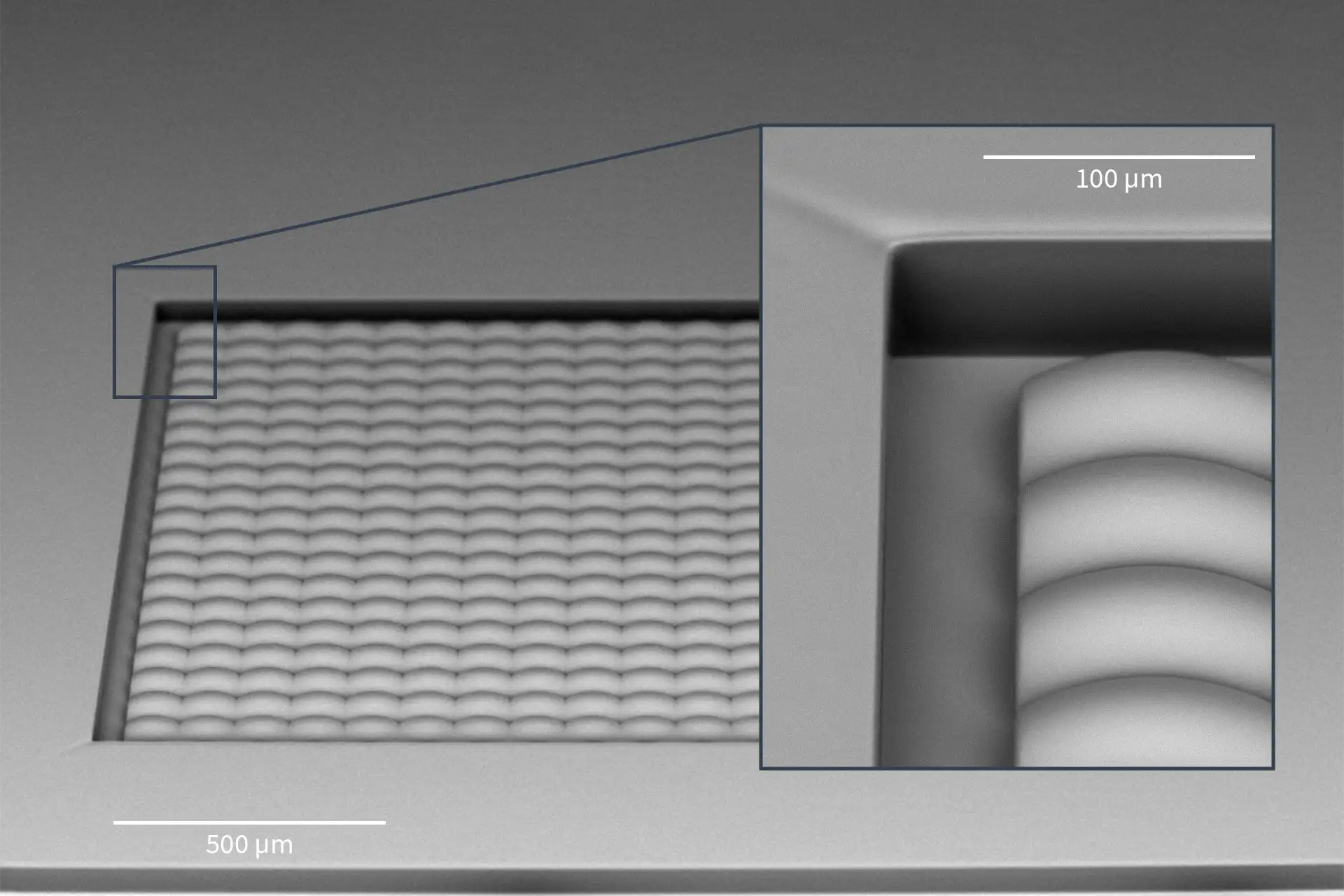
Two-Photon Polymerisation (TPP) has evolved into a disruptive tool in micro and macro fabrication for the realization of novel applications in various fields such as photonics, biomedicine, life sciences, and mechanics. Multiphoton Optics’ universal LithoProf3D-GSII TPP platform offers great possibilities when it comes to the realization of complex structures ranging from 1D to 3D. This webinar focusses on exemplarily applications of the technology in combination with the advantages of the LithoProf3D-GSII.
Speaker: Dr. Benedikt Stender, CEO at Multiphoton Optics GmbH
Thursday, August 26th, 8am CEST
NanoFrazor – A Nanolithography Tool for 2D & 3D Devices
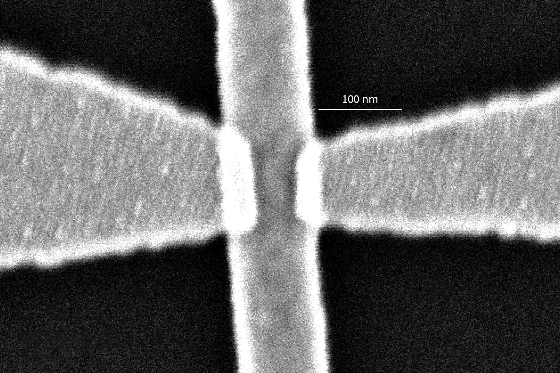
NanoFrazor lithography systems were developed as a first true alternative or extension to standard mask-less nanolithography methods like electron beam lithography (EBL). In contrast to EBL they are based on thermal scanning probe lithography (t-SPL). Here a heatable ultra-sharp probe tip with an apex of a few nm is used for patterning and simultaneously inspecting complex nanostructures.
The application range for this new nanolithography technique is very broad. The webinar will include examples for high-quality metal contacting of 2D materials, tuning photonic molecules, generating nanofluidic devices and generating spintronic circuits. Some of these applications have been enabled only due to the various unique capabilities of NanoFrazor lithography like the absence of damage from a charged particle beam.
Speaker: Dr. Nils Goedecke, Technical Sales Expert at Heidelberg Instruments Nano


