NanoFrazor Scholar – a tabletop system for thermal scanning probe lithography – made a long journey from Zurich to the Westlake University in Hangzhou, China. Upon arrival at its destination – Dr Xiaorui Zheng’s lab of Advanced Lithography for Opto-Electronic Nanochips (ALIEN) – it was unpacked, assembled, installed and successfully tested within 24 hours. The check after unpacking showed that all components worked properly. After its assembly and remote installation, the Scholar performed according to all specifications and solidly passed the acceptance test. It was our second remote installation in China since travel restrictions due to COVID-19.
An important reason why our remote installations go so smoothly is the support of our local partner Quantum Design China. They do a great job in helping customers to unpack, to connect the hardware and with everything else that needs to be done on-site. After the installation, the experts of Heidelberg Instruments’ Nano team trained the new users via video conferencing.
“I am very happy with the performance of the Scholar. Particularly because the installation was done remotely in such a record time, and the site acceptance test was completed without any problems.,” says Dr Zheng. “Any research instrument installation is a challenge during the COVID-19 pandemic. But the teams of HI Nano and QD China made it happen by working together closely both onsite and remotely.”
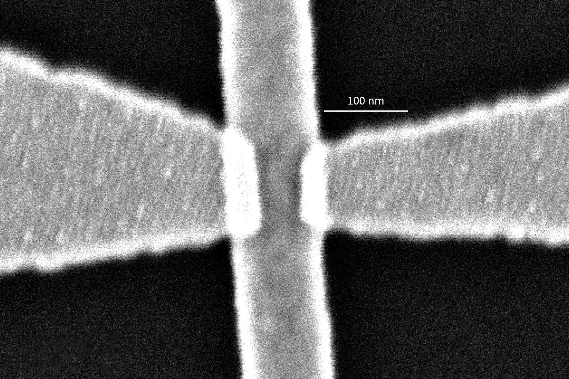
Sample fabrication began immediately after the installation, SAT, and the training. “We started patterning electrodes on 2D materials and it works pretty well – as expected”, Dr Zheng shared with us. “By now, the NF Scholar is fully integrated into our research. I also like the NanoFrazor software a lot: It is powerful, easy to use, and very smart in finding the right parameter during the calibration. It lowers the learning threshold for beginners very much.”
Dr Zheng is an expert in thermal scanning probe lithography, as he was working with the NanoFrazor Explore installed in Prof. Elisa Riedo’s laboratory at the New York University for a few years. Now he has established his own group at the Westlake University, where he plans to use the NanoFrazor Scholar to explore optoelectronic nanochips on emerging nanomaterials.
Research details can be explored on his group website.
News cover image: While taking a break from work, Dr Zheng has patterned a 3D nanoscale photo of the new Westlake University campus, where the Scholar will be moved to at the end of this year. In this image, 1 um corresponds to about 30 m, and one can distinguish even the balloons released during the campus opening ceremony (lower left corner).


