Scanning Tunnelling Microscopy (STM) relies on quantum tunnelling for imaging and manipulation of objects on atomic scale. It is one of the most precise techniques developed by physicists in the last century. 35 years after its conception, we see STM finding its way to applications beyond purely fundamental science.
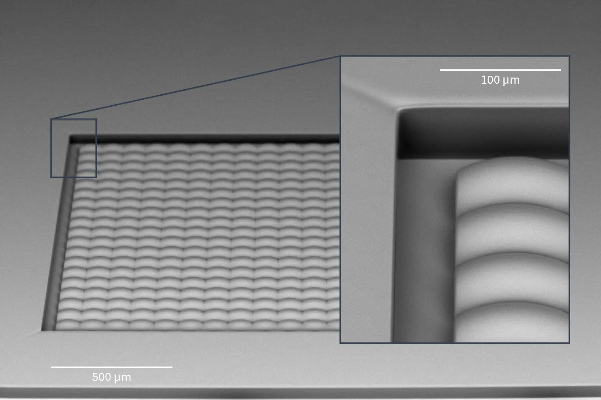
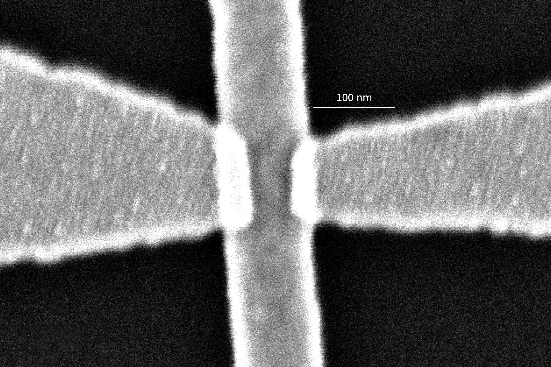
One of the pioneers of STM technology, Robert Wolkow, is a professor at the University of Alberta, Canada. His team has developed a simple way to make atomic-scale electronics. Locally removing Hydrogen atoms using a very sharp tip leaves dangling bonds. Prof. Wolkow and his team form a circuit using these dangling bonds. Behind this seemingly simple technique, there are several highly sophisticated steps: making the tip atomically sharp, detecting, and correcting mistakes, and, finally, merging the devices that are just a few atoms in size, with the macroscopic world, so they can do what conventional electronics cannot. Prof. Wolkow is a co-founder of Quantum Silicon, a start-up aiming to produce industrially relevant atomic scale devices, such as very fast and low-energy analog-to-digital Converters. For scaling up the production and the fabrication of contacts from the smallest dimensions of the device to micron-scale contacts, Quantum Silicon will be beta-testing the decapede (10-tip) write head of the NanoFrazor, which is soon to be released widely.
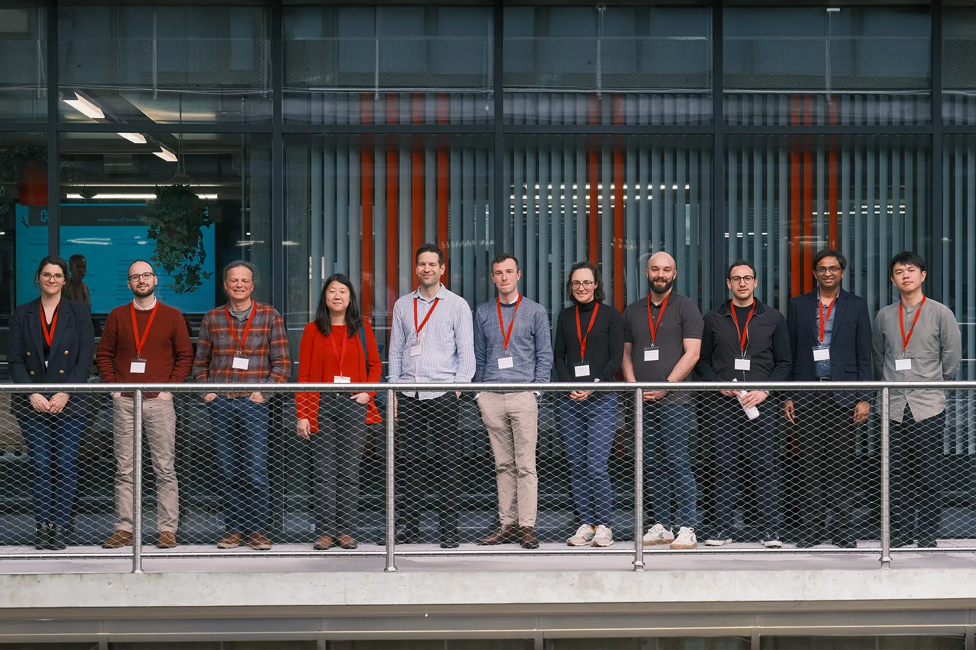
Prof. Wolkow told The Lithographer about his work and the struggles associated with the ambition to make smallest quantum devices “from the future” relevant to today’s technology. (Download the magazine to read the interview, p. 34)
Read this edition in our libray:
Select “The Lithographer” in the Category filter.