


Exciting news! At Kyoto University Nanotechnology Hub one MPO 100 3D microprinting system and one MLA 150 maskless lithography system have been successfully installed. This

A look back on the 8th Thermal Probe Workshop We were delighted to host a community of nanotechnology experts, fabrication researchers, rising stars and innovative
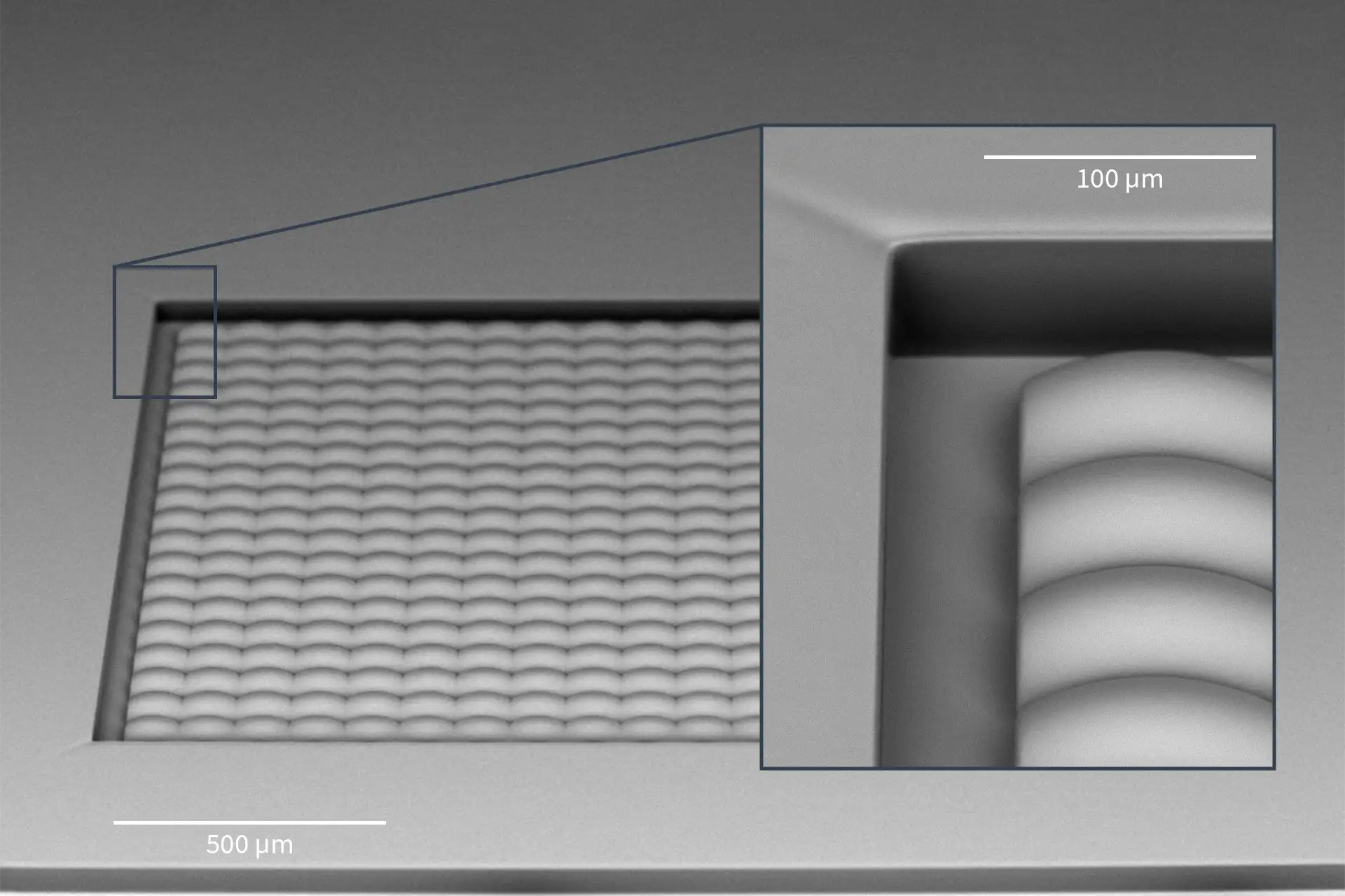
Achieve high throughput and resolution. Despite its unique capacity for three-dimensional fabrication with minimal feature sizes below 100 nm, achieving high throughput with Two-Photon Polymerization
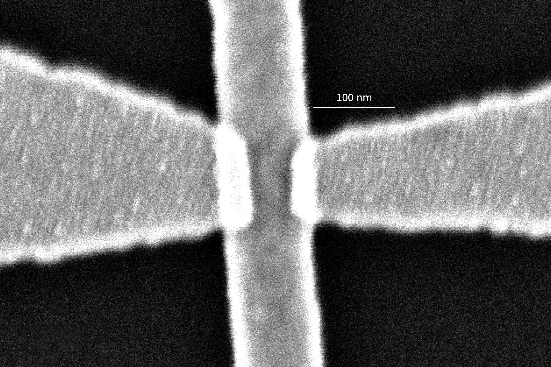
Discover our two Application Notes covering this topic: “Bilayer Lift-Off for NanoFrazor Lithography”“Ultra-High Resolution Pattern Transfer on NanoFrazor Lithography” In our recent application notes, we