Advanced Packaging
Wafer Level Packaging and System-In-Package
-
Description
-
The final stage of semiconductor device fabrication for electronics manufacturing involves Advanced Packaging of the integrated circuit (IC) to encapsulate it in a supporting case, known as a “package”. This package provides support for the electrical contacts that connect the IC to a circuit board. Different integrated circuits in the semiconductor industry require various packaging types based on parameters like size, power dissipation, field-operating conditions, and costs. Advanced Packaging technologies include BGA, Flip-Chip, CSP, LGA, and PGA, as well as multi-chip modules, systems-in-package, and heterogeneous integration, which offer higher integration densities than conventional PCBs.
These packaging methods offer different benefits such as speed, cost, functionality, and ease of integration for system designers. Depending on the packaging method and technical requirements, various materials need to be structured to implement the necessary fan-out and mapping of the IC contact pads. These materials, including silicon (TSVs), polymers, ceramics, and metals, all play a vital role in flexible and high-resolution lithography.
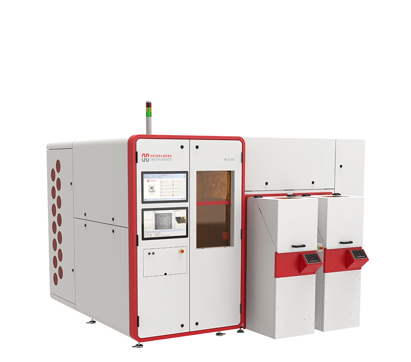
Heidelberg Instruments’ VPG+ and MLA 300 systems are designed for flexible production applications and offer high throughput, automatic distortion compensation, and auto-focus following for substrates with low planarity. These systems can structure various materials to implement the required fan-out and mapping of IC contact pads, allowing for the production of high-quality Advanced Packages that meet different packaging requirements for various integrated circuits in the semiconductor industry.
Find out more about the systems by visiting their product pages listed below.
-
Requirements
-
High throughput to reduce production time and cost
High availability and reliability to maximize uptime
High resolution (1 - 2 µm) for devices and back-end processes
High CD uniformity to ensure device consistency
High alignment accuracy to optimize yield
Accomodating various substrate materials, warpage, thicknesses, and sizes
Automatic distortion correction to compensate for distortions introduced by the different materials and the bonded devices
-
Solutions
-
Simultaneous exposure
of up to 4 million pixels for production grade throughput (MLA300)Fast setup time & flexibility
for small and medium production batchesAutomatic distortion correction
to increase yield by compensating distortions from other fabrication stepsField-proven technology
for high availability, manufacturing stability and reliability
The final stage of semiconductor device fabrication for electronics manufacturing involves Advanced Packaging of the integrated circuit (IC) to encapsulate it in a supporting case, known as a “package”. This package provides support for the electrical contacts that connect the IC to a circuit board. Different integrated circuits in the semiconductor industry require various packaging types based on parameters like size, power dissipation, field-operating conditions, and costs. Advanced Packaging technologies include BGA, Flip-Chip, CSP, LGA, and PGA, as well as multi-chip modules, systems-in-package, and heterogeneous integration, which offer higher integration densities than conventional PCBs.
These packaging methods offer different benefits such as speed, cost, functionality, and ease of integration for system designers. Depending on the packaging method and technical requirements, various materials need to be structured to implement the necessary fan-out and mapping of the IC contact pads. These materials, including silicon (TSVs), polymers, ceramics, and metals, all play a vital role in flexible and high-resolution lithography.
Heidelberg Instruments’ VPG+ and MLA 300 systems are designed for flexible production applications and offer high throughput, automatic distortion compensation, and auto-focus following for substrates with low planarity. These systems can structure various materials to implement the required fan-out and mapping of IC contact pads, allowing for the production of high-quality Advanced Packages that meet different packaging requirements for various integrated circuits in the semiconductor industry.
Find out more about the systems by visiting their product pages listed below.
High throughput to reduce production time and cost
High availability and reliability to maximize uptime
High resolution (1 - 2 µm) for devices and back-end processes
High CD uniformity to ensure device consistency
High alignment accuracy to optimize yield
Accomodating various substrate materials, warpage, thicknesses, and sizes
Automatic distortion correction to compensate for distortions introduced by the different materials and the bonded devices
Simultaneous exposure
of up to 4 million pixels for production grade throughput (MLA300)
Fast setup time & flexibility
for small and medium production batches
Automatic distortion correction
to increase yield by compensating distortions from other fabrication steps
Field-proven technology
for high availability, manufacturing stability and reliability
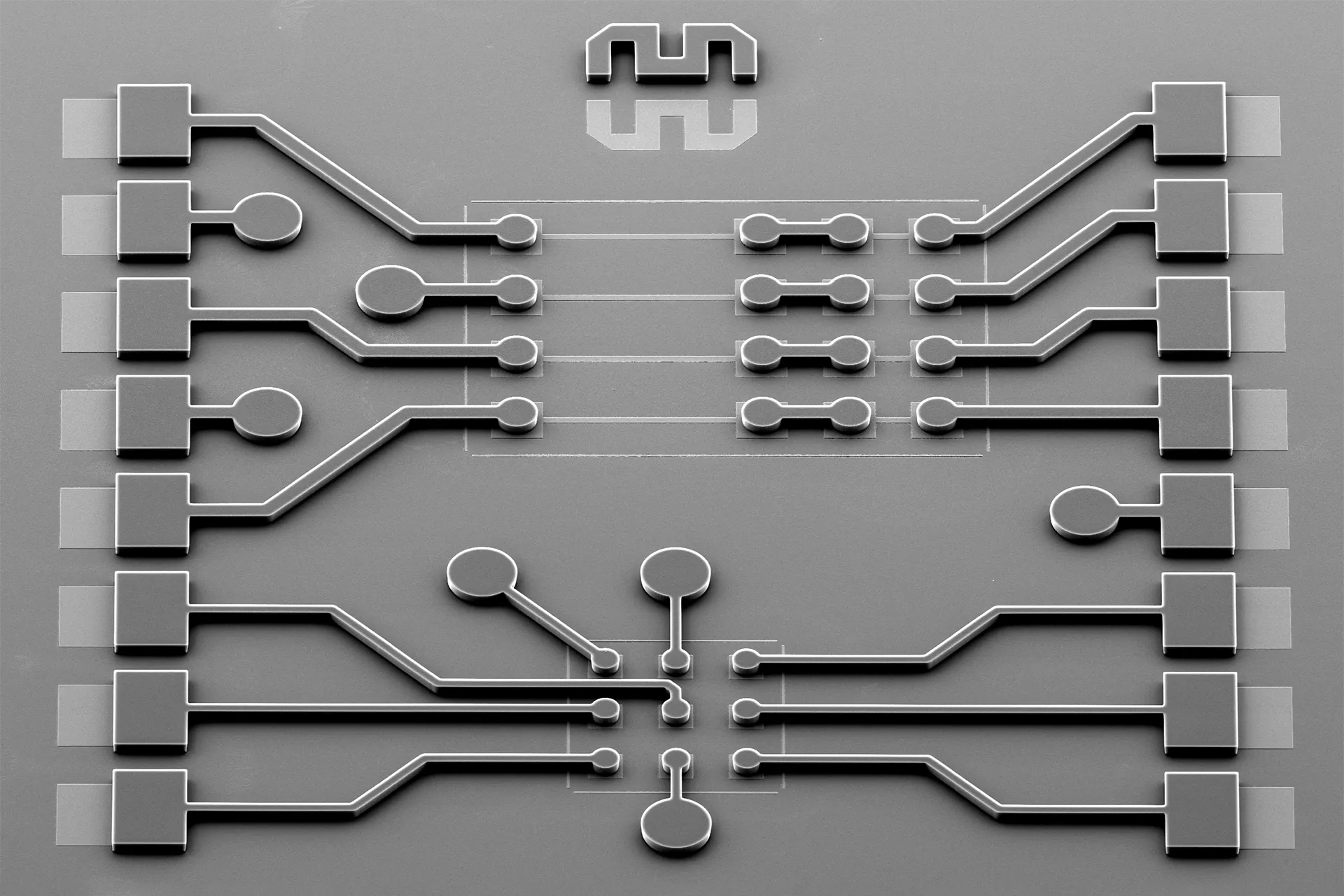
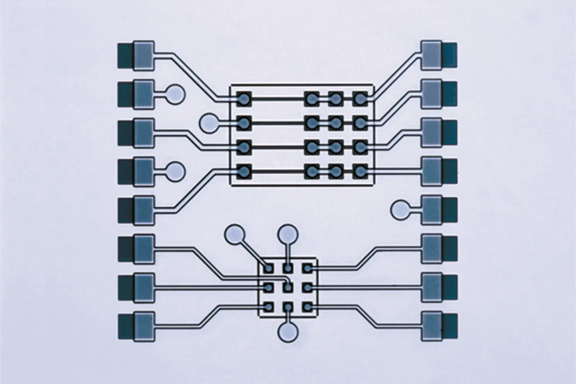
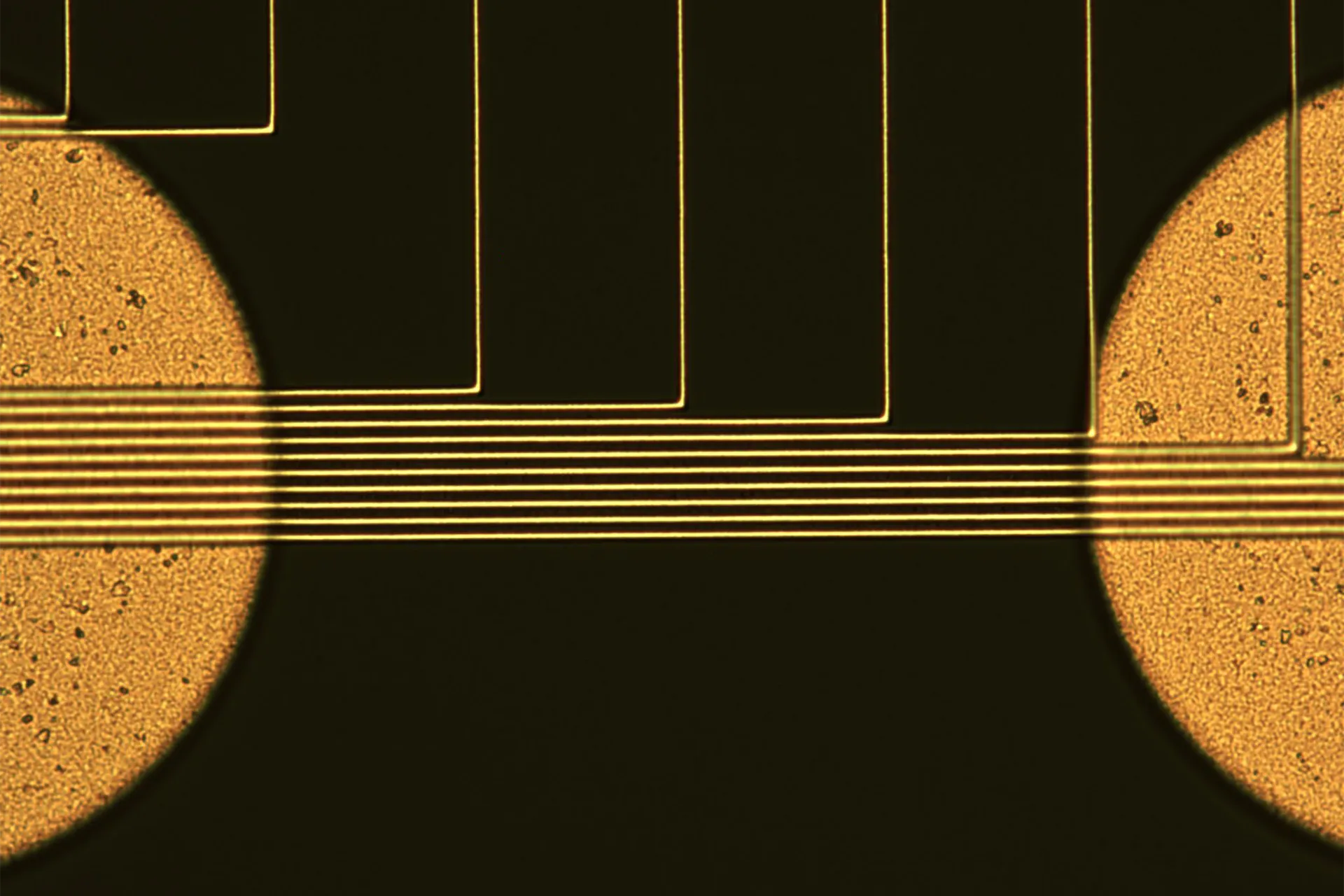
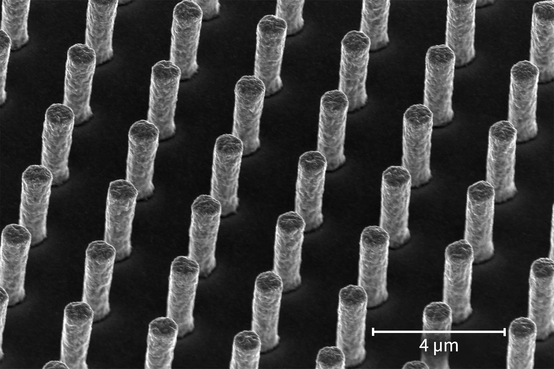
Application images
(Courtesy of Fraunhofer IZM, Panel Level Consortium 2.0)
(Courtesy of Fraunhofer IZM - ASSID)
*Redistribution Line / ** Fan-out Wafer-Level Packaging
(Courtesy of Fraunhofer IZM, Panel Level Consortium 2.0)
suitable Systems
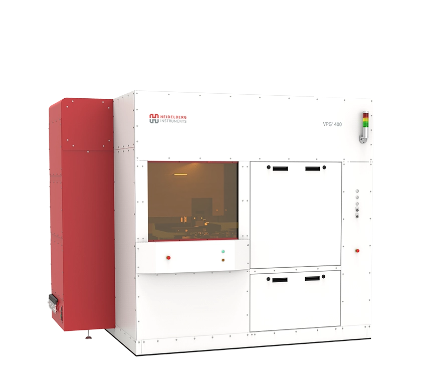
VPG+ 200 / VPG+ 400
- Volume Pattern Generator
A production tool for standard photomasks and microstructures in i-line resists.
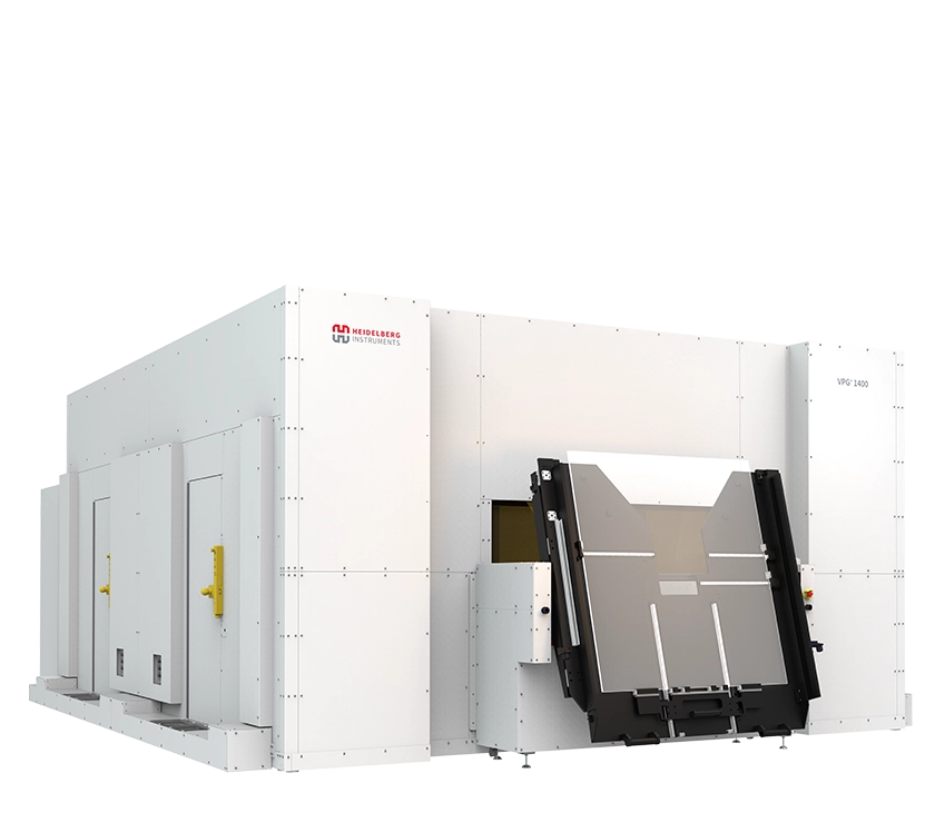
VPG+ 800 / VPG+ 1400
- Volume Pattern Generator
Photomask production on large substrates, perfect for display applications.