Optimized for industrial manufacturing, ensuring high throughput and seamless production line integration
-
Product Description
-
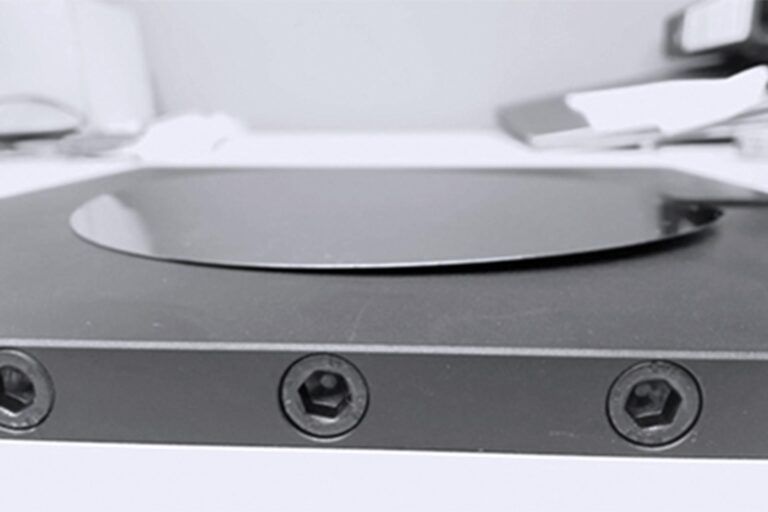
The Maskless Aligner MLA 300 provides high throughput, a simplified workflow, and integration with manufacturing execution systems (MES). This tool is used for the production of sensors and sensor ICs, MEMS, and microfluidic devices. Other applications include discrete electronic components, analog and digital ICs, ASICs, power electronics, OLED displays, and advanced packaging.
The MLA 300 achieves the highest optical quality and precision. The standard exposure module achieves a minimum feature size of 1.5 µm. Writing modes for higher throughput and higher resolution are on our roadmap. The MLA 300 features full automation with customizable loading options, software designed for production environments, and patented substrate tracking technology.
The MLA 300 reduces production costs and effort by overcoming the requirement for mask procurement, verification, and management. Operating costs benefit from a long-lifetime exposure laser (estimated 10 years at 24/7 production) and fewer consumables. Modularity enables fast maintenance, replacement, or repair. Real-time autofocus compensates for substrate warp or corrugations, ensuring flawless patterning. Maskless lithography allows per-die pattern corrections and serialization for full tracing of product characteristics, such as sensor calibration.
-
Product Highlights
-
Direct-write Lithography
No mask-related costs, effort, or security risksFlexibility
Direct writing in industrial production allows per-die pattern corrections, e.g. to react to distortions or process variations and serializationTime-saving
Shorter time from prototyping to production. Digital design management replaces conventional mask libraryExposure Quality
Optical compensation of scaling, rotation; patented substrate tracking technologyDynamic Autofocus
Superior critical dimensions (CD) uniformity on warped or corrugated substratesExposure Speed
300 x 300 mm2 in 19.5 minutesFull Facility Integration
Customizable automatic loader, substrate chuck including warped substrates, custom workflow “wizards” and interface with manufacturing execution systems (MES)User-friendly
SEMI-compliant user interface; customized workflow “wizards” for system operators -
Available Modules
-
Automated Loading Module
SEMI-standard BOLTS plane can be configured for open cassettes or Load Ports for FOUP. The number and configuration of ports can be selected and customized for round or rectangular substratesManufacturing Execution System (MES)
Integration Customizable workflow “wizards” to start exposure jobs, and integration to a central MES via SECS/GEM or OPC-UA protocolsBackside Alignment
Visual or through-wafer IR backside alignment available with 1 µm positioning accuracyExposure Wavelengths
High-power diode lasers with 7 W at 375 nm or 20 W at 405 nm with long lifetime are availableMultipurpose Vacuum Chuck
Customized vacuum chucks are available for applications with special substrates (e.g. warped panels)Service Contracts
Service contract grades for faster on-site support and participation in the spare parts pool
The Maskless Aligner MLA 300 provides high throughput, a simplified workflow, and integration with manufacturing execution systems (MES). This tool is used for the production of sensors and sensor ICs, MEMS, and microfluidic devices. Other applications include discrete electronic components, analog and digital ICs, ASICs, power electronics, OLED displays, and advanced packaging.
The MLA 300 achieves the highest optical quality and precision. The standard exposure module achieves a minimum feature size of 1.5 µm. Writing modes for higher throughput and higher resolution are on our roadmap. The MLA 300 features full automation with customizable loading options, software designed for production environments, and patented substrate tracking technology.
The MLA 300 reduces production costs and effort by overcoming the requirement for mask procurement, verification, and management. Operating costs benefit from a long-lifetime exposure laser (estimated 10 years at 24/7 production) and fewer consumables. Modularity enables fast maintenance, replacement, or repair. Real-time autofocus compensates for substrate warp or corrugations, ensuring flawless patterning. Maskless lithography allows per-die pattern corrections and serialization for full tracing of product characteristics, such as sensor calibration.
Direct-write Lithography
Flexibility
Time-saving
Exposure Quality
Dynamic Autofocus
Exposure Speed
Full Facility Integration
User-friendly
Automated Loading Module
Manufacturing Execution System (MES)
Backside Alignment
Exposure Wavelengths
Multipurpose Vacuum Chuck
Service Contracts
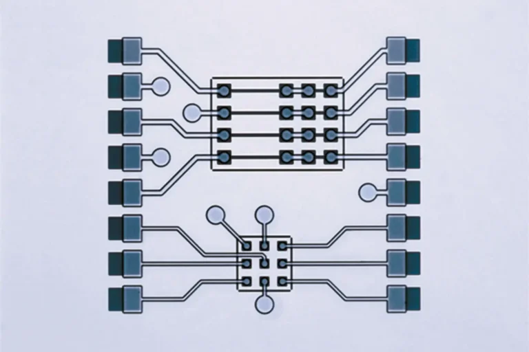
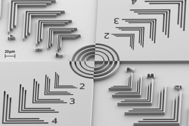
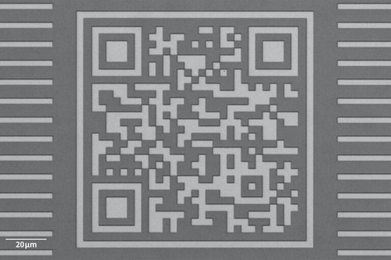
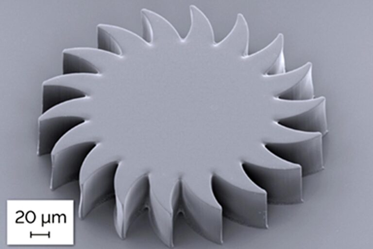
Customer applications


Why customers choose our systems
John McLean, Principle Process Development Engineer
Centre for Process Innovation (CPI)
Sedgefield, England
Technical Data
| Writing performance | |
|---|---|
| Minimum lines and spaces [µm] | 2 |
| Minimum feature size [µm] | 1.5 |
| CD uniformity [3σ, nm] | 200 |
| Edge roughness [3σ, nm] | 80 |
| Stitching [3σ, nm] | 120 |
| 2nd layer alignment [3σ, nm] | 500 |
| Backside alignment [3σ, nm] | 1000 |
| Exposure time per module (100 x 100 mm² at 80 mJ/cm² and 405 nm laser wavelength) | 2.75 min |
| Maximum write speed with one module at 405 nm laser wavelength | 4615 mm²/min |
| System features | |
|---|---|
| Light source | High-power diode lasers at 375 nm or 405 nm |
| Maximum substrate size | 300 x 300 mm² |
| Maximum exposure area | 300 x 300 mm² |
| Substrate thickness | 0.1 - 10 mm |
| Modular environmental chamber | Temperature stability ± 0.1°C |
| Real-time autofocus | Optical and/or pneumatic autofocus |
| Autofocus dynamic range | Up to 150 µm |
| Alignment | Advanced alignment; backside alignment optional |
| Automation | Automatic wafer handling and pre-alignment |
| System dimensions (excluding loader) | |
| Height × width × depth | 1980 mm x 1200 mm x 2310 mm |
| Weight | 2600 kg |
| Installation requirements | |
| Electrical | 400 VAC, 50/60 Hz, 16 A |
Please note
Specifications depend on individual process conditions and may vary according to equipment configuration. Write speed depends on pixel size and write mode. Design and specifications are subject to change without prior notice.