Working with materials at the nano- and micro-scale requires attention to the impact of pattern and device dimensions on material properties.
Direct-Write Lithography offers a flexible method for modifying and shaping materials at these scales, enabling control of a range of physical properties. Heidelberg Instruments’ DWL and MLA series use Direct-Write Laser Lithography to create micro-scale patterns, structures, and textures, as well as contacts for electronic devices and measurements.
Additionally, Thermal Scanning Probe-Lithography (t-SPL) can be used to initiate material modifications on the nanoscale, with the added ability to apply local heating. The NanoFrazor provides a highly precise and versatile tool for lithography, allowing ultra-fast heating, cooling, and high local pressure to be applied to materials at the nanoscale, opening up access to states of matter that may not be accessible macroscopically.
These Direct-Write Lithography techniques can be used to study and control the physical properties of materials, with potential applications in fields such as high-performance electronics, energy storage, and water purification. As pattern and device dimensions continue to shrink, direct write lithography offers a promising path towards continued advancement in nanotechnology.
Listed below are some images related to Materials Science and the systems suited for this application.
Used to generate modifications and new materials locally on the nanoscale (NanoFrazor)
Accurate overlay
Used to align electrodes onto nanoscale materials without alignment marks (NanoFrazor)
No clean room required
High-resolution lithography using novel materials
Non-invasive lithography
Used to preserve physical properties of sensitive materials that would otherwise be damaged or destroyed by irradiation with charged particles or contact with air (glovebox solutions)
Working with materials at the nano- and micro-scale requires attention to the impact of pattern and device dimensions on material properties.
Direct-Write Lithography offers a flexible method for modifying and shaping materials at these scales, enabling control of a range of physical properties. Heidelberg Instruments’ DWL and MLA series use Direct-Write Laser Lithography to create micro-scale patterns, structures, and textures, as well as contacts for electronic devices and measurements.
Additionally, Thermal Scanning Probe-Lithography (t-SPL) can be used to initiate material modifications on the nanoscale, with the added ability to apply local heating. The NanoFrazor provides a highly precise and versatile tool for lithography, allowing ultra-fast heating, cooling, and high local pressure to be applied to materials at the nanoscale, opening up access to states of matter that may not be accessible macroscopically.
These Direct-Write Lithography techniques can be used to study and control the physical properties of materials, with potential applications in fields such as high-performance electronics, energy storage, and water purification. As pattern and device dimensions continue to shrink, direct write lithography offers a promising path towards continued advancement in nanotechnology.
Listed below are some images related to Materials Science and the systems suited for this application.
Patterning on arbitrary materials
Non-invasive lithography
Localized heating
Precise temperature control
Thermal conversion
Used to generate modifications and new materials locally on the nanoscale (NanoFrazor)
Accurate overlay
Used to align electrodes onto nanoscale materials without alignment marks (NanoFrazor)
No clean room required
High-resolution lithography using novel materials
Non-invasive lithography
Used to preserve physical properties of sensitive materials that would otherwise be damaged or destroyed by irradiation with charged particles or contact with air (glovebox solutions)
Application images
Microscale columns with flat tops (the tops are 2x2 um) patterned using a MLA 150 Maskless Aligner.
(Courtesy of EPFL Center for Micronanotechnology)
Directed self-assembly of PS-b-PMMA lamellae on top of a 25 nm HP NanoFrazor pattern (right)
and without a guiding pattern (left). (Courtesy of CNM-IMB Barcelona, Spain)
Metal contacts with vanishingly small Schottky barriers fabricated using the NanoFrazor.
On single-layer CVD-grown MoS2. (Courtesy of Prof. Elisa Riedo, NYU, see Nat.Electr.2019)
Heated NanoFrazor tip creates ferroelectric PZT nanostructures by local crystallization of an amorphous sol-gel precursor material. (Courtesy of Riedo group, NYU, published by Kim et al. in Adv. Mat. 2011)
SEM image of 100-nm-wide squares patterned by NanoFrazor and subsequently
ion milled into a rough iron oxide film.
Single Ni nanowires used to investigate Co-Ni alloy magneto-thermopower
and magneto-resistance. (Courtesy of Tim Boehnert, University of Hamburg)
NanoFrazor can be used for high-resolution direct removal of certain materials; here a perovskite
crystal (inset) was patterned. (Courtesy of Hemayyet Uddin (MCN, Melbourne), in cooperation with Heidelberg Instruments Nano)
Thermal quenching of a thermochromic supramolecular polymer to obtain fluorescence contrast via disaggregation of excimer-forming moieties. (Courtesy of LMIS1 at EPFL, published by Zimmermann et al. in ACS Appl. Mat. & Int. 9, 2017)
suitable Systems
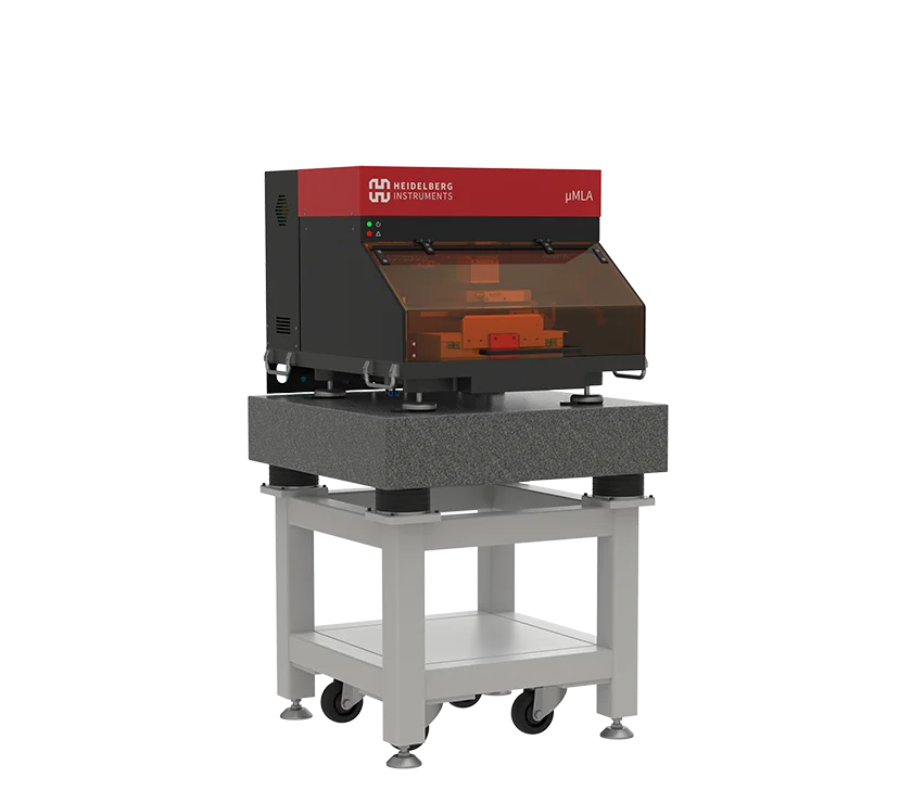
µMLA
Maskless Aligner
Configurable and compact tabletop maskless aligner with raster scan and vector exposure modules.
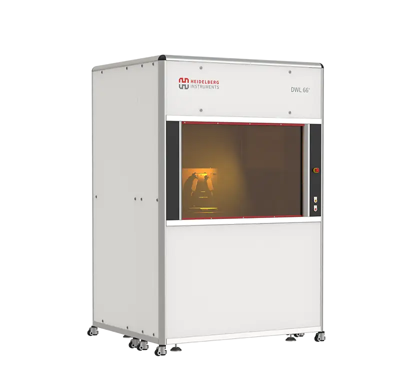
DWL 66+
Direct Write Laser Lithography System
Our most versatile system for research and prototyping with variable resolution and wide selection of options.
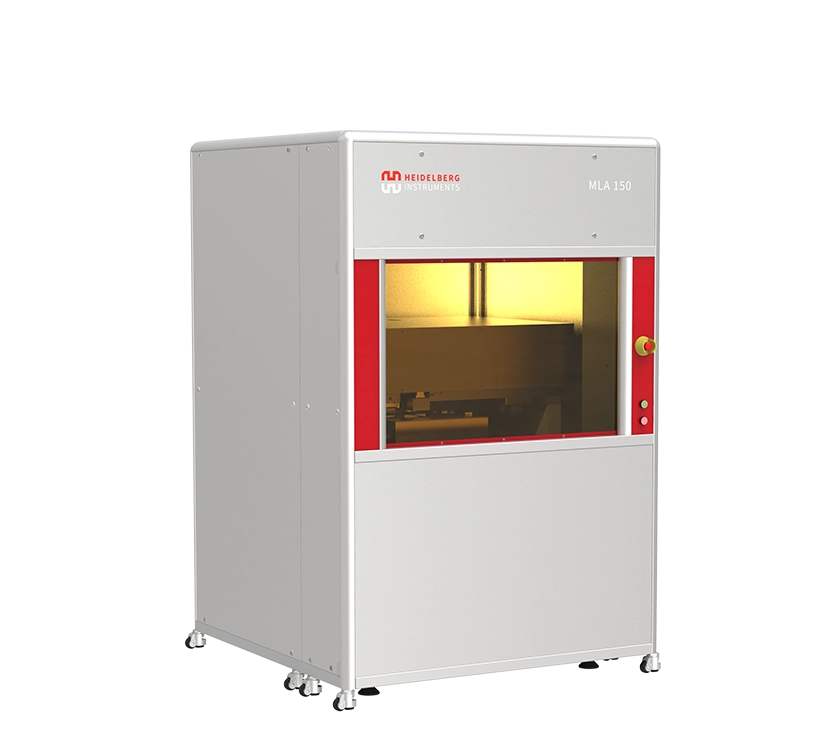
MLA 150
Maskless Aligner
The fastest maskless tool for rapid prototyping, the alternative to the mask aligners. Perfect for standard binary lithography.
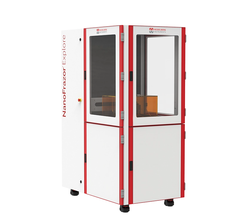
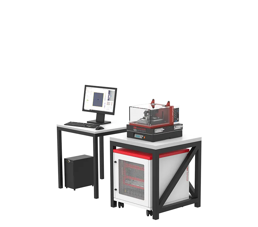
NanoFrazor Explore
Thermal Scanning Probe Lithography System
Thermal scanning probe lithography tool with direct laser sublimation and grayscale modules. Excellent alternative to e-beam lithography tools.