Chips Powering the Data Age
When the SEMICON Europa 2022 gets underway next month at the Messe München in Munich, Germany, the role played by semiconductor chips will be the main theme coursing through the program. The four-day SEMICON Europa 2022 themed “Chips Powering the Data Age” is co-located with electronica in Munich and will summon technology experts and industry leaders for insights into the latest technology, materials and process innovations enabling the next-generation of semiconductor devices.
Maskless Laser Lithography Solutions for Semiconductor and Photonics Industry
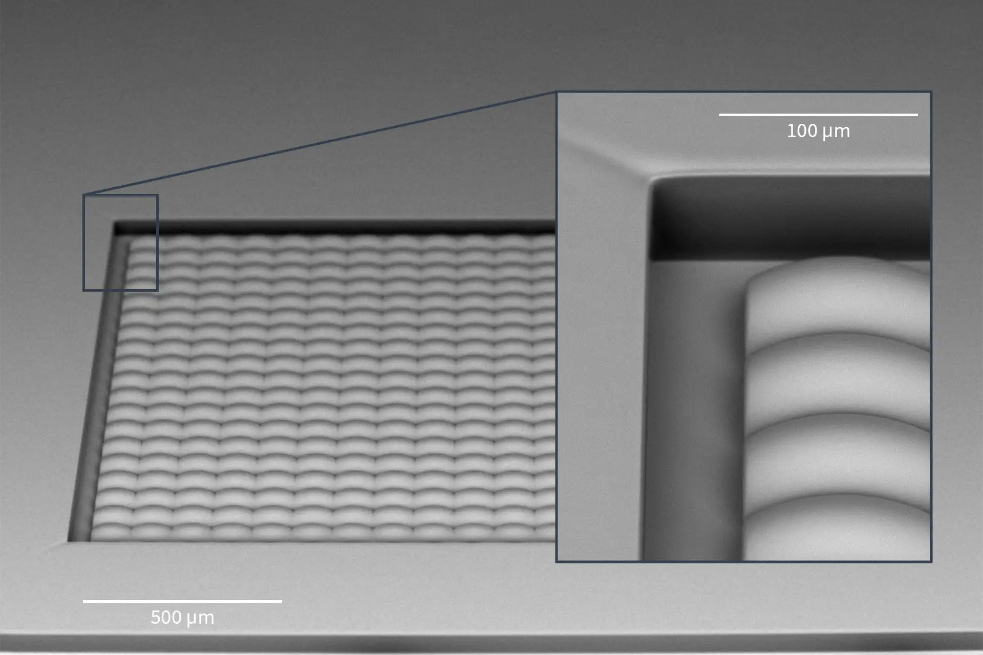
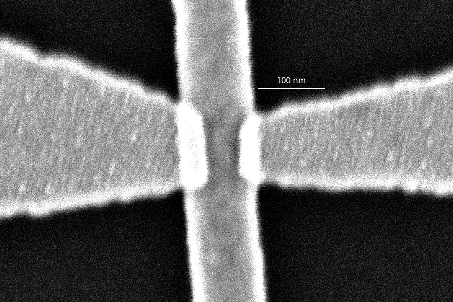
Many of our modern everyday life achievements in communications, information processing, healthcare, transportation and industrial manufacturing are based on groundbreaking innovations in the field of semiconductors and photonics. High precision laser lithography systems have been essential to make these innovations possible and continue to play a key role in the patterning process in chip manufacturing to bring semiconductor and photonic devices to the next level.
As a world leading provider of high precision photolithography systems, maskless laser lithography and nanofabrication systems, Heidelberg Instruments will present its innovative lithography solutions dedicated for pilot to volume manufacturing applications in semiconductor, photonics and photomask industries.
With over three decades of photolithography and semiconductor experience, Heidelberg Instruments can support you to take full advantage of maskless direct write lithography to fulfill the patterning needs for the fabrication of electronic and optoelectronic components.
Visit us and the co-exhibitors of the LAB14 joint booth C1465 to learn more about significant technological advances from Heidelberg Instruments for semiconductor and photonics lithography applications, such as the MLA 300 Maskless Aligner specifically designed to integrate into production facilities. This state-of-the-art maskless aligner combines all the benefits provided by maskless lithography into one industrial solution: Rapid design customizations, processing of warped substrates, and a customizable loading system allowing fully automating production with a resolution down to 2 µm lines and spaces.
Are you interested? Schedule a meeting and get a free ticket
Click on the button below to schedule a meeting with us and receive your free ticket for SEMICON Europa in Munich. We will be happy to arrange an appointment to discuss your lithography-specific applications and projects in the semiconductor industry.