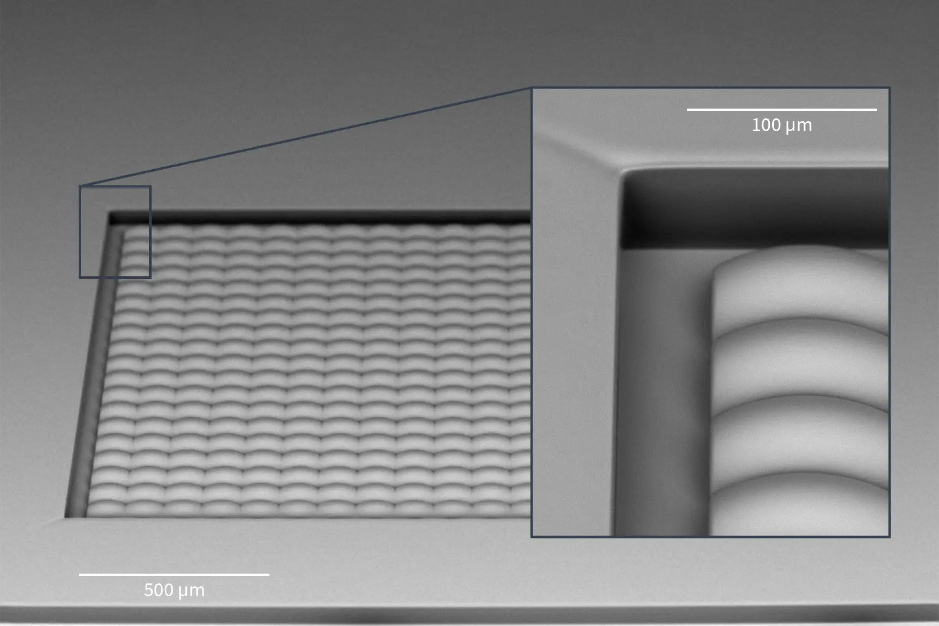
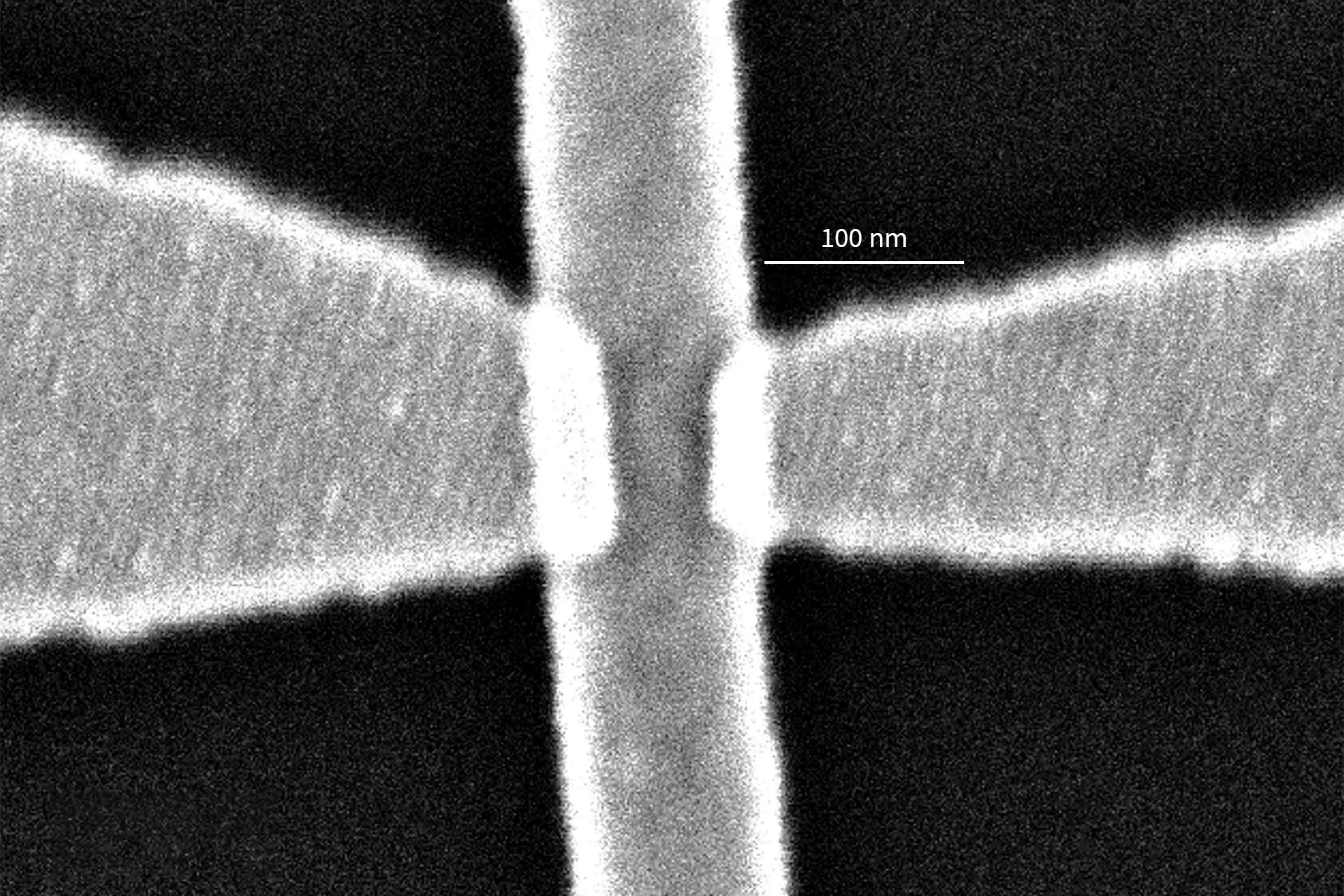
NanoFrazor can be used to locally induce heat-driven phase changes. Dr Ann-Katrin U. Michel and her colleagues from ETH Zürich and RWTH Aachen University are exploring this capability. They proposed a new technique for fabricating near-infrared metasurfaces with feature sizes far below the diffraction limit. Their results were recently published in Advanced Optical Materials.
Phase-change materials such as GeTe, which was the material used in this work, have distinctly different properties depending on whether they are in their crystalline or amorphous state. The heat from the NanoFrazor’s tip drives crystallization of a small volume of the material under the tip. The resulting array of few-nm-sized crystalline dots in amorphous GeTe would significantly change the wavelength at which the resulting metasurface absorbs the light.
In this work, the authors designed a perfect absorber for the near-infrared spectral range. These wavelengths are typically used in telecommunications, so such devices could prove very useful for currently existing technology. A similar approach can also be used for other optics and biosensing applications.
Blog
Novel Metasurfaces Made of Phase-Change Materials
Share:
Categories
Archives
Social Media
Popular Posts
10 years of NanoFrazor – history and outlook
Heidelberg Instruments celebrates 10 years of NanoFrazor
Related Posts
DWL 66+ Customer Satisfaction Survey
Customer satisfaction is our top priority and an important indicator to support customer-oriented development of our systems. For this reason and in order to guarantee the quality of our products and processes, we conduct customer surveys on a regular basis. Among the participants of our most recent survey on our DWL 66+ system we have
10 years of NanoFrazor – history and outlook
The commercialization of the NanoFrazor started in 2012. This article looks back at where the NanoFrazor came from, how it evolved over the last 10 years, and where it is heading now. The origins of Thermal Scanning Probe Lithography Already in the early 1990s, John Mamin and Dan Rugar from IBM Research Almaden, California showed
Heidelberg Instruments celebrates 10 years of NanoFrazor
Zurich, Switzerland / Heidelberg, Germany – Heidelberg Instruments Nano AG in Zurich, a subsidiary office of Heidelberg Instruments Mikrotechnik GmbH celebrated the 10-year anniversary of the commercialization of the NanoFrazor system series. The NanoFrazor is based on the Thermal Scanning Probe (t-SPL) technology and can be used for nanopatterning of quantum devices on 1D/2D materials,
MPO 100 goes Australia: ANFF-Q purchases 3D nanoprinter
Würzburg, Germany / Brisbane, Australia – The Australian National Fabrication Facility – Queensland Node (ANFF-Q) based at the University of Queensland, Australia has placed a purchase order for the recently launched Two-Photon Polymerization tool MPO 100. The system, developed by Multiphoton Optics GmbH and manufactured by its parent company Heidelberg Instruments Mikrotechnik GmbH, will provide