Heidelberg, March 30, 2022. Heidelberg Instruments has received a significant order from a leading semiconductor wafer-level packaging production company in Asia for its MLA 300 Maskless Aligner. With this order, Heidelberg Instruments has reached another important milestone towards the company’s goal of becoming a leading supplier of maskless lithography tools to the advanced wafer-level packaging industry.
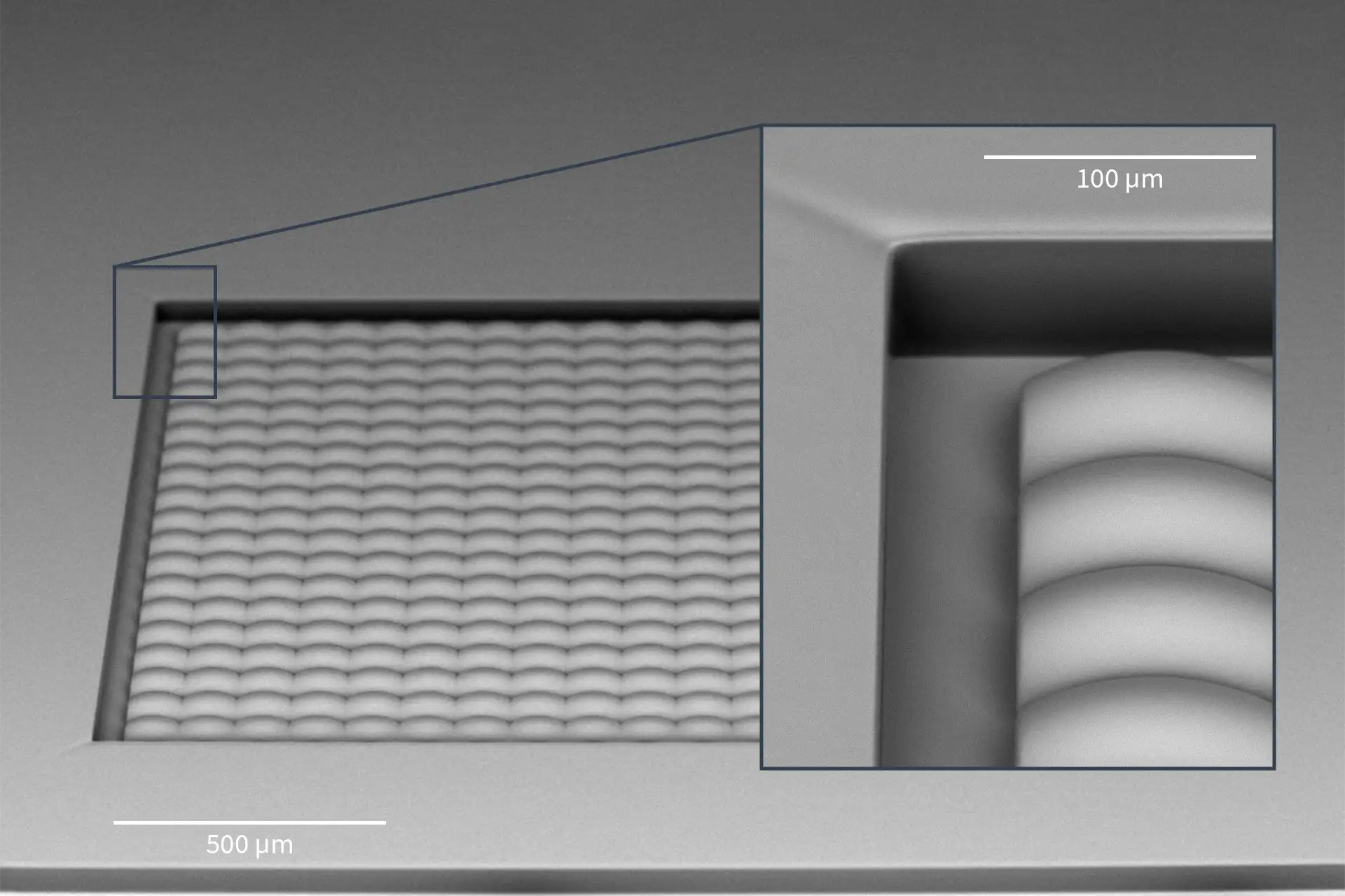
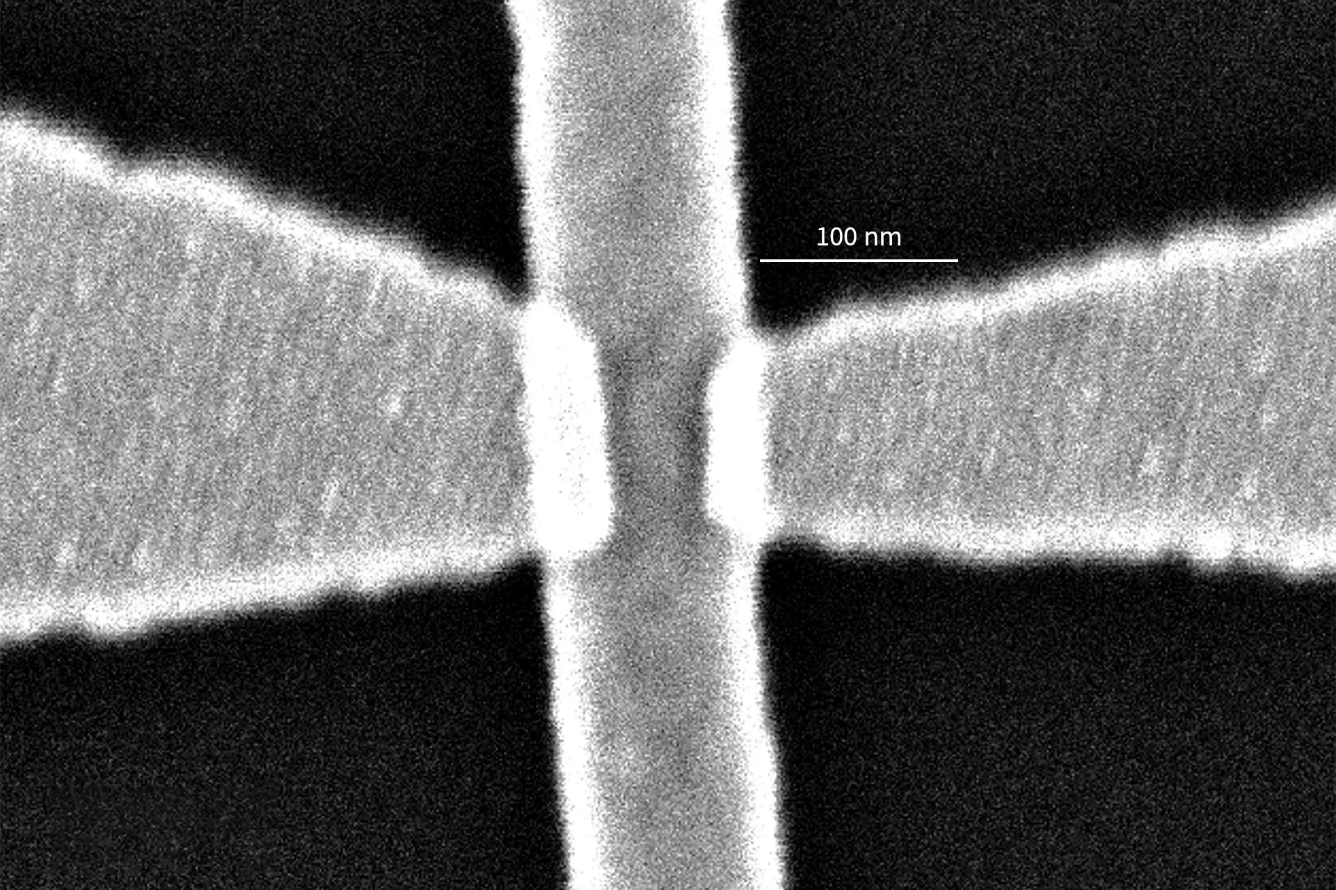
Optimized for industrial manufacturing, the MLA 300 Maskless Aligner features distinct benefits for the wafer-level technology: The flexibility of maskless lithography allows rapid design customizations, and even unique designs on each substrate. This is of particular use for chip packaging where mounted die shift and each panel is unique. Meeting these demands, the MLA 300 can be seamlessly integrated into wafer-level packaging production lines, fully automating wafer production with a resolution down to 2 µm lines and spaces. The MLA 300 reduces production costs and efforts by eliminating mask procurement, verification, and management requirements. Operating costs are reduced by utilizing a long-lifetime exposure laser and fewer consumables. Modularity enables fast maintenance, replacement, or repair. Real-time autofocus compensates substrate warp or corrugations for flawless patterning.
Since its market introduction at the end of 2019, the MLA 300 has received a terrific reception and has become a popular tool for the microfabrication industry. The MLA 300 comprises a customizable wafer handling system, customizable vacuum chucks, and a large autofocus compensation help account for challenges like warped substrates, and software designed for production environments.
“This latest order, by a leading advanced wafer packaging production group, is a big step forward for us and maskless lithography. With the MLA 300, Heidelberg Instruments has introduced the most innovative maskless lithography system for mid-volume wafer production and high-volume prototyping. So far, several fabrication groups globally have purchased and installed the MLA 300 tool, replacing their traditional lithography production platforms, such as mask aligners and steppers,” says Alexander Forozan, Head of Global Sales and Business Development, Heidelberg Instruments group of companies.
MLA 300 is a versatile tool for application areas such as advanced semiconductor packaging, IR sensors, MEMS, electronic probes, and high precision electronic components.
About Heidelberg Instruments
With over 35 years of experience and more than 1,200 installed systems, Heidelberg Instruments is one of the leading international players in the development and production of high-precision photolithography systems and nanofabrication tools. Heidelberg Instruments systems are installed in industrial and scientific facilities around the world. They are used for efficient direct writing, as well as for photomask fabrication for a wide range of industries – including semiconductors, quantum computing, photonics, 2D materials, IoT, and many related application fields.
Marketing and Communication Contact
Veronika Loose
Heidelberg Instruments Mikrotechnik GmbH
Mittelgewannweg 27
69123 Heidelberg
Tel. +49 931 908792 88
E-Mail: veronika.loose@heidelberg-instruments.com