
Ambipolar tellurium floating-gate devices enable nonvolatile memory with high retention, endurance, large on/off ratios, and reconfigurable excitatory–inhibitory synapses, achieving >90% accurate neuromorphic image recognition.
汎用性の高いモジュール式ナノリソグラフィツール
-
商品説明
-
NanoFrazor は、熱走査プローブリソグラフィー(t-SPL)の画期的な商用システムであり、さまざまな分野での高度な研究と革新を可能にするよう設計されています。 量子デバイス、1D/2D 材料、量子ドット、ジョセフソン接合、またはナノスケールデバイスアレイを研究する場合でも、NanoFrazor は比類のない精度と多用途性を提供します。 その機能は、グレースケールフォトニクス、ナノ流体構造、細胞成長のための生体模倣基板、熱による化学反応や物理的相変化による局所的な材料改質など、複雑な課題にも対応します。
主な特徴
- 高解像度ナノパターニング:NanoFrazor の心臓部には、複雑なナノ構造の書き込みと検査を同時に可能にする、超鋭利で加熱可能なプローブ・チップがある。自己補正パターニングは、クローズドループ・リソグラフィー(CLL)機能によって実現されます。この革新的な設計は、複雑なパターンや構造を作成するための比類のない精度を提供します。
- ダイレクトレーザー昇華(DLS)モジュール:DLSモジュールは、ナノおよびマイクロ構造を1つのステップで同じレジスト層に効率的に書き込むことを可能にすることにより、ファブリケーションを合理化します。この統合により、ワークフローが簡素化され、生産性が向上します。
- マーカーレスオーバーレイによるその場イメージング:NanoFrazor のインサイチュ・イメージング技術は、マーカーレス・オーバーレイを導入し、書き込まれたパターンとターゲット・パターンをリアルタイムで比較します。このユニークなCLL(Closed-Loop Lithography)機能は、複雑な2.5D(グレースケール)形状を作成するための2nm以下の垂直精度を保証し、描画プロセス中に即座にパラメータを調整することができます。
- 10チップによる並列書き込み:Decapede機能は、NanoFrazor の定評ある精度を維持しながら、10本のヒータブル・チップによる並列書き込みを可能にし、スループットを大幅に向上させます。この機能は、大面積のパターニングや時間に制約のあるアプリケーションに最適です。
- モジュール式でアップグレード可能な設計:NanoFrazorのモジュラー・プラットフォームは、特定の研究ニーズやラボ環境を満たすための広範なカスタマイズを可能にします。パターニング・モード、ハウジング・オプション、ソフトウェア・モジュールは、最大限の柔軟性と機能性を実現するためにカスタマイズすることができます。研究の進展に応じて、NanoFrazor は追加モジュールでアップグレードすることができ、長期的な適応性を保証します。
- 包括的なプロセスサポート:IBM Research Zürich および Heidelberg Instruments Nano での 20 年以上にわたる研究開発により、NanoFrazor のユーザーコミュニティはハードウェアおよびソフトウェアの継続的な進歩の恩恵を受けています。ユーザーは、エッチングやリフトオフなどのパターントランスファープロセスに関するベストプラクティスやプロトコルの包括的なライブラリにアクセスでき、さまざまな用途で最適な結果を確保できます。
アプリケーション
- 量子デバイス:量子コンピューティングや高度な電子アプリケーションのための精密なナノ構造を作成する。
- 1次元/2次元材料:グラフェン、遷移金属ジカルコゲナイド、その他の2次元材料上のナノ構造をパターン化し、修正する。
- フォトニクス:光学システムにおける正弦波グレーティングや位相板のようなグレースケール形状に対して、2 nm未満の垂直精度を実現。
- バイオテクノロジー:細胞増殖のためのバイオミメティック基板を開発し、生物学的および化学的分析のためのナノ流体構造を作製。
- 局所的な材料改質:化学反応や相変化など、局所的な熱駆動プロセスを可能にし、材料科学における革新的な研究を実現します。
NanoFrazor は、先進的な熱走査プローブリソグラフィーを世界中の研究者や技術者に利用可能にすることで、ナノファブリケーションを革新します。最先端の機能、モジュール式デザイン、幅広い応用範囲により、画期的な研究や技術革新に欠かせないツールとなっています。
NanoFrazor についてさらに詳しく知るには、専用ウェブサイト nanofrazor.com をご覧ください。 システムを構成し、NanoFrazor がどのようにあなたの研究を新たな高みへと引き上げるかを体験してください。
-
製品ハイライト
-
熱走査プローブリソグラフィー
ナノパターニングへの新たなアプローチで、他では実現不可能なアプリケーションを可能にする高解像度
複雑な形状でもナノ構造のパターニングが容易;最小横方向形状15nm、垂直方向分解能2nmダメージフリーリソグラフィー
荷電粒子によるダメージなし、近接効果なし、クリーンなリフトオフ互換性
リフトオフ、エッチングなど、すべての標準的なパターン転写方法。- 当社の “レシピブック “で利用可能な知識リソースとベストプラクティスユニークなサーマルカンチレバー
マイクロヒーターと距離センサーを内蔵し、交換が容易で費用対効果に優れる精密なオーバーレイとステッチ
マーカレスオーバーレイとステッチ精度 25 nm指定、10 nm以下のオーバーレイを表示インシチュイメージング
パターン化された構造特性のリアルタイム可視化低所有コスト
クリーンルーム、真空ポンプ、高価な消耗品が不要スクリプト
カスタム・オペレーションの容易な自動化 -
利用可能なモジュール
-
レーザー昇華モジュール
波長405nmのCWファイバーレーザーにより、粗い構造も同一露光ステップで高スループットに露光。デカペード
パラレル・ライティング10のヒント独立型ハウジング
3層防音、優れた防振|PC制御による温湿度モニタリング、ガス流量調整|(寸法185cm x 78cm x 128cm、重量650kg)フルグローブボックス・インテグレーション
制御された環境でナノリソグラフィが可能なグローブボックスへの統合グレースケール・ソフトウェア・モジュール
2 nm以下の垂直分解能で2.5Dパターニングが可能自動オーバーレイ・ソフトウェア・モジュール
25nmの精度で既存の地形にマーカーレスで自動オーバーレイスマート・スプリッティング・ソフトウェア・モジュール
大きなレイアウトの処理とフィールドの順序の最適化ダイナミックな局所温度変調
熱による局所的な材料改質を利用した熱化学用途向け
NanoFrazor は、熱走査プローブリソグラフィー(t-SPL)の画期的な商用システムであり、さまざまな分野での高度な研究と革新を可能にするよう設計されています。 量子デバイス、1D/2D 材料、量子ドット、ジョセフソン接合、またはナノスケールデバイスアレイを研究する場合でも、NanoFrazor は比類のない精度と多用途性を提供します。 その機能は、グレースケールフォトニクス、ナノ流体構造、細胞成長のための生体模倣基板、熱による化学反応や物理的相変化による局所的な材料改質など、複雑な課題にも対応します。
主な特徴
- 高解像度ナノパターニング:NanoFrazor の心臓部には、複雑なナノ構造の書き込みと検査を同時に可能にする、超鋭利で加熱可能なプローブ・チップがある。自己補正パターニングは、クローズドループ・リソグラフィー(CLL)機能によって実現されます。この革新的な設計は、複雑なパターンや構造を作成するための比類のない精度を提供します。
- ダイレクトレーザー昇華(DLS)モジュール:DLSモジュールは、ナノおよびマイクロ構造を1つのステップで同じレジスト層に効率的に書き込むことを可能にすることにより、ファブリケーションを合理化します。この統合により、ワークフローが簡素化され、生産性が向上します。
- マーカーレスオーバーレイによるその場イメージング:NanoFrazor のインサイチュ・イメージング技術は、マーカーレス・オーバーレイを導入し、書き込まれたパターンとターゲット・パターンをリアルタイムで比較します。このユニークなCLL(Closed-Loop Lithography)機能は、複雑な2.5D(グレースケール)形状を作成するための2nm以下の垂直精度を保証し、描画プロセス中に即座にパラメータを調整することができます。
- 10チップによる並列書き込み:Decapede機能は、NanoFrazor の定評ある精度を維持しながら、10本のヒータブル・チップによる並列書き込みを可能にし、スループットを大幅に向上させます。この機能は、大面積のパターニングや時間に制約のあるアプリケーションに最適です。
- モジュール式でアップグレード可能な設計:NanoFrazorのモジュラー・プラットフォームは、特定の研究ニーズやラボ環境を満たすための広範なカスタマイズを可能にします。パターニング・モード、ハウジング・オプション、ソフトウェア・モジュールは、最大限の柔軟性と機能性を実現するためにカスタマイズすることができます。研究の進展に応じて、NanoFrazor は追加モジュールでアップグレードすることができ、長期的な適応性を保証します。
- 包括的なプロセスサポート:IBM Research Zürich および Heidelberg Instruments Nano での 20 年以上にわたる研究開発により、NanoFrazor のユーザーコミュニティはハードウェアおよびソフトウェアの継続的な進歩の恩恵を受けています。ユーザーは、エッチングやリフトオフなどのパターントランスファープロセスに関するベストプラクティスやプロトコルの包括的なライブラリにアクセスでき、さまざまな用途で最適な結果を確保できます。
アプリケーション
- 量子デバイス:量子コンピューティングや高度な電子アプリケーションのための精密なナノ構造を作成する。
- 1次元/2次元材料:グラフェン、遷移金属ジカルコゲナイド、その他の2次元材料上のナノ構造をパターン化し、修正する。
- フォトニクス:光学システムにおける正弦波グレーティングや位相板のようなグレースケール形状に対して、2 nm未満の垂直精度を実現。
- バイオテクノロジー:細胞増殖のためのバイオミメティック基板を開発し、生物学的および化学的分析のためのナノ流体構造を作製。
- 局所的な材料改質:化学反応や相変化など、局所的な熱駆動プロセスを可能にし、材料科学における革新的な研究を実現します。
NanoFrazor は、先進的な熱走査プローブリソグラフィーを世界中の研究者や技術者に利用可能にすることで、ナノファブリケーションを革新します。最先端の機能、モジュール式デザイン、幅広い応用範囲により、画期的な研究や技術革新に欠かせないツールとなっています。
NanoFrazor についてさらに詳しく知るには、専用ウェブサイト nanofrazor.com をご覧ください。 システムを構成し、NanoFrazor がどのようにあなたの研究を新たな高みへと引き上げるかを体験してください。
熱走査プローブリソグラフィー
ナノパターニングへの新たなアプローチで、他では実現不可能なアプリケーションを可能にする
高解像度
複雑な形状でもナノ構造のパターニングが容易;最小横方向形状15nm、垂直方向分解能2nm
ダメージフリーリソグラフィー
荷電粒子によるダメージなし、近接効果なし、クリーンなリフトオフ
互換性
リフトオフ、エッチングなど、すべての標準的なパターン転写方法。- 当社の “レシピブック “で利用可能な知識リソースとベストプラクティス
ユニークなサーマルカンチレバー
マイクロヒーターと距離センサーを内蔵し、交換が容易で費用対効果に優れる
精密なオーバーレイとステッチ
マーカレスオーバーレイとステッチ精度 25 nm指定、10 nm以下のオーバーレイを表示
インシチュイメージング
パターン化された構造特性のリアルタイム可視化
低所有コスト
クリーンルーム、真空ポンプ、高価な消耗品が不要
スクリプト
カスタム・オペレーションの容易な自動化
レーザー昇華モジュール
波長405nmのCWファイバーレーザーにより、粗い構造も同一露光ステップで高スループットに露光。
デカペード
パラレル・ライティング10のヒント
独立型ハウジング
3層防音、優れた防振|PC制御による温湿度モニタリング、ガス流量調整|(寸法185cm x 78cm x 128cm、重量650kg)
フルグローブボックス・インテグレーション
制御された環境でナノリソグラフィが可能なグローブボックスへの統合
グレースケール・ソフトウェア・モジュール
2 nm以下の垂直分解能で2.5Dパターニングが可能
自動オーバーレイ・ソフトウェア・モジュール
25nmの精度で既存の地形にマーカーレスで自動オーバーレイ
スマート・スプリッティング・ソフトウェア・モジュール
大きなレイアウトの処理とフィールドの順序の最適化
ダイナミックな局所温度変調
熱による局所的な材料改質を利用した熱化学用途向け
お客様のアプリケーション

作製プロセスについては、アプリケーションノートをお読みください。

(L. Shani*, J. Chaaban* et al 2024 Nanotechnology 35 255302)


(提供:Yannik Glauser, ETH Zürich)


製造プロセスについて学ぶには、アプリケーションノートをお読みください。


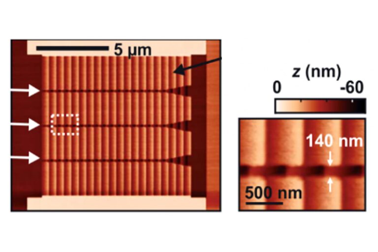
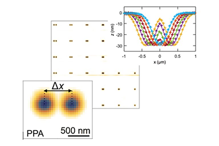
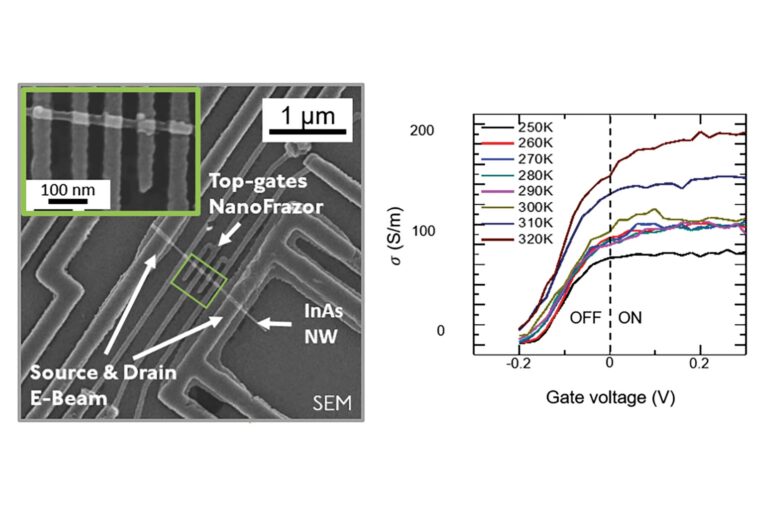
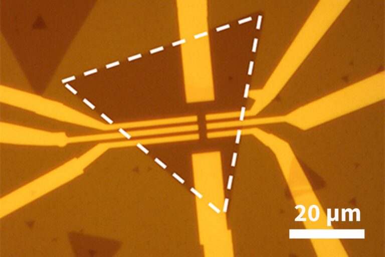
製造プロセスについて詳しくは、アプリケーションノートをお読みください。

お客様が当社のシステムを選ぶ理由
NanoFrazor が提供するクローズドループリソグラフィー機能を非常に高く評価しています。これは、高精度リソグラフィー、オーバーレイ、ステッチングなど、低次元材料応用のさまざまな用途に非常に役立っています。また、システム使用に関するあらゆる要望に対して、NanoFrazor サポートチームから24時間以内に迅速かつプロフェッショナルな対応をいただいており、感謝しています。
Xiaorui Zheng、助教、研究代表者
ウェストレイク大学
中国・杭州市
Nanofrazorは、ナノリソグラフィー用の単一のコンパクトな装置に、独自の機能群を統合しています。特に注目すべきは、2次元材料に対するマーカーレスなオーバーレイおよびステッチング(低損傷)、3次元グレースケール・ナノリソグラフィー、そして材料の直接的な熱変換・改質機能です。
Francesco Buatier de Mongeot、実験凝縮系物理学教授
ジェノヴァ大学 物理学部
イタリア、ジェノヴァ
技術データ
| サーマル・プローブ ライティング | ダイレクトレーザー 昇華 | ||
|---|---|---|---|
| シングルチップ | デカペード | ||
| パターニング性能 | |||
| 最小構造サイズ [nm] | 15 | 15 | 600 |
| 最小ラインとスペース[ハーフピッチ、nm] | 25 | 25 | 1000 |
| グレースケール/3D解像度(PPAのステップサイズ)[nm] | 2 | 2 | - |
| 最大書き込みフィールドサイズ[X μm x Y μm] | 60 x 60 | 60 x 60 | 60 x 60 |
| フィールドステッチ精度(マーカーレス、その場撮像を使用)[nm] | 25 | 25 | 600 |
| オーバーレイ精度(マーカーレス、その場イメージングを使用) [nm] | 25 | 25 | 600 |
| 書き込み速度(標準スキャン速度)[mm/s] | 1 | 1 | 5 |
| 書き込み速度(50nmピクセル)[μm²/min] | 1000 | 10 000 | 100 000 |
| トポグラフィー画像性能 | |||
| 横方向の画像分解能(フィーチャーサイズ) [nm] | 10 | ||
| 垂直分解能(トポグラフィ感度) [nm] | <0.5 | ||
| イメージング速度(@50nm分解能)[μm²/分] | 1000 | 10 000 | - |
| 基本システムの特徴 | |
|---|---|
| 基板サイズ | 1 x 1 mm² ~ 100 x 100 mm² (制限付きで 150 x 150 mm² も可能)
厚さ:最大 10 mm |
| 光学顕微鏡 | デジタル分解能0.6μm、回折限界2μm、視野1.0mm×1.0mm、オートフォーカス |
| 磁気カンチレバーホルダー | 高速(<1分)で正確なチップ交換 |
| 防振 | アクティブ防振ステージ |
| オプションのシステム機能/モジュール性 | |
| ダイレクトレーザー昇華 | レーザー光源と光学系波長405nm CWファイバーレーザー、300mW、最小焦点サイズ1.2μm レーザーオートフォーカス:NanoFrazorカンチレバーの距離センサーを使用。 |
| デカペード | パラレル・ライティング10のヒント |
| 独立型ハウジング | 3層防音構造、優れた防振性(> 98% @ 10 Hz)|PC制御による温度・湿度モニタリングおよびガス流量調整|(寸法185 cm × 78 cm × 128 cm/重量650 kg) |
| グローブボックスとの完全統合 | 制御された環境でナノリソグラフィが可能なグローブボックスへの統合 |
| NanoFrazor カンチレバーの特徴(シングルチップとデカペデの両方) | |
| 統合コンポーネント | チップヒーター、トポグラフィーセンサー、静電アクチュエーター |
| 先端形状 | <半径10nm、長さ750nmの円錐形チップ |
| チップヒーター温度範囲 | 25 °C – 1400 °C (<1 K の設定点分解能) |
| ベースシステムの寸法と設置条件 | |
| 高さ×幅×奥行き | テーブルトップユニット:44 cm x 40 cm x 45 cm コントローラー: 84 cm x 60 cm x 56 cm |
| 重量 | テーブルトップユニット50 kg コントローラー:80 kg |
| 電源入力 | 1 x 110または220 V AC、10 A |
| ソフトウェアの特徴 | |
| GDSおよびビットマップのインポート、256階調のグレースケール、トポグラフィー画像解析およびオーバーレイ描画、チップ描画とレーザー描画のミックス&マッチ、完全自動キャリブレーションルーチン、Pythonスクリプト対応 |
ご注意
仕様は個々のプロセス条件によって異なり、装置の構成によっても変動する場合があります。書き込み速度はピクセルサイズおよび書き込みモードによって異なります。設計および仕様は予告なく変更される場合があります。
関連出版物
| Title | Date | Publisher | Summary | Link |
|---|---|---|---|---|
| Nanoscale Spatial Tuning of Superconductivity in Cuprate Thin Films via Direct Laser Writing | July 23, 2026 | Advanced Functional Materials | Direct laser writing with the Heidelberg Instruments DWL 66⁺ and NanoFrazor enables nanoscale oxygen-stoichiometry tuning in YBCO, precisely controlling superconducting properties and enabling scalable functional nanostructures. | |
| Fourier Pixels for Bidirectional Light Control | June 24, 2026 | nature | Fourier pixels use miniaturized diffractive structures and plasmonic waves to both generate and fully characterize optical wavefronts (amplitude, phase, polarization), enabling compact bidirectional light control. | |
| Broadband, compact, and training-free optical processors for parallel image classification | February 21, 2026 | arXiv Physics/Optics | Compact, training-free optical processor using Fourier surfaces enables broadband, parallel image classification with up to 20 simultaneous computations, achieving high accuracy and scalable, low-power performance. | |
| Engineered Strain in 2D Materials by Direct Growth on Deterministically Patterned Grayscale Topographies | February 10, 2026 | Advanced Science | Strain is engineered during 2D growth on grayscale topographies, achieving controlled 0–0.5% uni- and multiaxial tensile strain in MoS2 without transfer, enabling direct integration into nanoelectronics. | |
| Beta Site Installation of NanoFrazor with Parallelization Capabilities at EPFL | January 20, 2026 | Heidelberg Instruments | Following the successful introduction of the modular NanoFrazor nanolithography system in 2024, Heidelberg Instruments is proud to announce the installation of the newest NanoFrazor at EPFL. | |
| Strained 2D Semiconductor Lateral Heterojunctions via Grayscale Thermal-Scanning Probe Lithography | January 12, 2026 | Small | Locally strained 2D semiconductor lateral heterojunctions are created by maskless grayscale thermal-Scanning Probe Lithography, enabling tunable asymmetric electrical behavior in MoS₂–Au nanoarrays for nanoelectronic and sensing applications. | |
| Beyond Binary Patterning: Polypropylene Carbonate as a Versatile Thermal Resist for High-Fidelity Grayscale Nanofabrication | January 8, 2026 | Microsystems & Nanoengineering (nature) | Polypropylene carbonate enables high-resolution t-SPL nanopatterning via controlled thermal decomposition, achieving 50 nm lateral, sub-nanometer vertical resolution and grayscale pattern transfer for photonic and nanoelectronic fabrication. | |
| Top-Down Fabrication of Silicon Nanowire Field-Effect Transistors Using Thermal Scanning Probe Lithography | December 16, 2025 | ACS Applied Nano Materials | Hybrid t-SPL and photolithography fabricate Si nanowire FETs with precise dimensional control, reproducible liquid-gate characteristics, and low-cost processing for biosensing applications. | |
| Gradient Electronic Landscapes in van der Waals Heterostructures | December 3, 2025 | Nano Letters | Thermal scanning probe lithography patterns nanometer-precise topographies in hBN-encapsulated graphene, enabling periodic electric-field modulation and tailored quantum transport potentials beyond planar device geometries. | |
| Defect Engineering in β‐Bi2 SeO5 /Bi2 O2 Se Heterostructures for High‐Resolution Phototransistor Arrays | November 24, 2025 | Advanced Materials | Defect-engineered β-Bi2SeO5/Bi2O2Se heterojunctions suppress vacancies, enable type-II charge separation, and achieve high-responsivity phototransistors and high-resolution arrays for advanced optoelectronics. | |
| Three-dimensional nanoscale control of magnetism in crystalline Yttrium Iron Garnet | October 30, 2025 | nature communications | Focused UV laser writing enables three-dimensional, non-destructive anisotropy engineering in crystalline YIG, tuning spin-wave band structures, localization, and non-reciprocity for advanced magnonic and magneto-optic devices. | |
| Independent Control of Quality Factor and Circular Dichroism via Intrinsic Chiral Plasmonic Bound States in the Continuum | September 27, 2025 | Laser & Photonics Reviews | 3D symmetry-broken plasmonic metasurfaces enable visible quasi-BIC resonances with independently tunable circular dichroism and Q-factors, achieving high chiroptical performance via nanoscale height-controlled architectures. | |
| Manipulating Anisotropy of Second Harmonic Generation in NbOI2 via Precise Strain Engineering | September 10, 2025 | Advanced Functional Materials | Precisely oriented strain engineering in NbOI2 enhances second harmonic generation up to 19-fold, quantitatively linking strain direction with nonlinear susceptibility and enabling tunable 2D ferroelectric optoelectronics. | |
| Josephson Junction Device Fabrication with the NanoFrazor | August 18, 2025 | Heidelberg Instruments Nano | High-resolution, damage-free NanoFrazor lithography enables fast and reliable fabrication of Josephson junctions for quantum and nanoelectronics applications. | |
| High-Resolution Lift-Off Process with the NanoFrazor | August 18, 2025 | Heidelberg Instruments Nano | This application note describes the NanoFrazor’s high-resolution lift-off process for creating sub-100 nm metal features with low line edge roughness using thermal lithography. | |
| Confinement-Enhanced Core–Shell Avalanche Photodetectors | July 8, 2025 | ACS Nano | A SiO2-passivated Si nanowire/graphene nanoresonator enhances 1550 nm absorption and confined avalanche multiplication, achieving 56.6 A/W responsivity and 2.6×10⁴ gain for CMOS-compatible NIR photodetection. | |
| Nanofabrication of All-Dielectric Metasurfaces through Pulsed Thermal Scanning Probe Lithography | July 2, 2025 | Scientific Reports | Pulsed thermal scanning probe lithography enables sub-10 nm patterning on insulating silica without conductive layers, advancing all-dielectric metasurface fabrication and material compatibility in nanofabrication. | |
| Noninvasive Deterministic Nanostructures Lithography on 2D Transition Metal Dichalcogenides | June 23, 2025 | Advanced Engineering Materials | Noninvasive t-SPL enables high-resolution nanolithography on transparent substrates, enabling tunable plasmonic nanostructures for applications in nanophotonics, sensing, and thermoplasmonics. | |
| Hybrid-Contact Engineering for Enhanced P-Type Performance in WSe2 Field-Effect Transistors | June 17, 2025 | Nanotechnology | Hybrid edge-top contacts in WSe2 FETs mitigate Fermi-level pinning, boosting p-type conduction, lowering contact resistance and Schottky barriers, enabling efficient complementary post-silicon electronics. | |
| Fourier-Tailored Light–Matter Coupling in van der Waals Heterostructures | May 27, 2025 | ACS Nano | Fourier-patterned hBN/WS2 van der Waals heterostructures enhance exciton–waveguide coupling, enabling exciton-polariton formation near strong coupling for advanced optoelectronic and quantum devices. | |
| Reconfigurable Artificial Synapses Based on Ambipolar Environmentally Stable Tellurium for Neuromorphic Computing | May 24, 2025 | ACS Applied Materials & Interfaces | ||
| Multifunctional Logic-in-Memory Circuits Based on Reconfigurable WSe2 Transistors via Enhanced Ambipolarity | May 15, 2025 | ACS Nano | Scanning probe lithography enhances ambipolar WSe2 transport, enabling nonvolatile reconfigurable memory, transistor, and diode modes with ~10¹⁰ on/off ratios, realizing ambient logic-in-memory circuits. | |
| Diffraction of Light from Optical Fourier Surfaces | April 28, 2025 | ACS Photonics | Precisely fabricated optical Fourier surfaces show measured diffraction matching electrodynamic simulations, outperforming binary profiles and scalar models, enabling accurate Fourier-spectrum engineering for advanced holography and optical computing. | |
| Combination of Thermal Scanning Probe Lithography and Directed Self-Assembly of Block Copolymers | April 24, 2025 | SPIE. Digital Library | Combining thermal scanning probe lithography with block copolymer self-assembly enables sub-20 nm, high-density quantum device patterning, achieving depth-amplified nanoholes and sub-10 nm placement accuracy. | |
| Strategies to Extend Resolution Limits for Direct Write Lithography | April 23, 2025 | SPIE. Digital Library | This presentation introduces methods for optimizing various direct-writing lithography systems from Heidelberg Instruments to push the resolution limit for smaller structures in collaboration with IMS Chips Germany. | |
| Detection of Dynamic Temperature Modulation using a Thermal Scanning Probe Lithography (t-SPL) System | April 8, 2025 | AIP Publishing | Thermal scanning probe lithography enables nanoscale thermal diffusivity measurement via localized periodic heating and temperature-wave phase analysis, achieving 10–100 nm resolution without miniaturized sensing. | |
| Dynamic BIC in Customizable Hydrogel Metagratings for Advanced Information Security | March 27, 2025 | Advanced Functional Materials | Water-responsive hydrogel metagratings with grayscale thermal patterning enable humidity-tunable q-BIC resonances for multistage visible optical encryption and concealed Morse-code decryption. | |
| Toward Phonon-Limited Transport in Two-Dimensional Transition Metal Dichalcogenides by Oxygen-Free Fabrication | February 24, 2025 | ACS Nano | An oxygen-free fabrication approach boosts MoS2 and WS2 FET mobility toward phonon limits, achieving record values and showing oxygen chemisorption critically degrades 2D transistor performance. | |
| Hybrid Contact for High‐Performance MoS2 Transistors via Hard‐Mask Scanning Probe Lithography | January 20, 2025 | Advanced Materials | Hard-mask scanning probe lithography enables hybrid contacts for MoS2 FETs, improving carrier injection, reducing contact resistance and Schottky barriers, achieving high on-current, large on/off ratios, and ~18 nm patterning. | |
| Selective Placement of Functionalised DNA Origami via Thermal Scanning Probe Lithography Patterning | November 4, 2024 | Materials Advances | Thermal scanning probe lithography organized functionalized DNA origami into predefined nanoarrays with single-molecule precision, positioning gold nanoparticles and quantum dots for heterofunctional bionanotechnology applications. | |
| Quantitative Mapping of Smooth Topographic Landscapes Produced by Thermal Scanning-Probe Lithography | October 28, 2024 | Nature Protocols | This work introduces FunFit, open-source software fitting analytical functions to SPM data, enabling precise fabrication, transfer, and feedback analysis of tSPL-patterned polymer and hBN nanoscale landscapes. | |
| Nanoscale-Localized Multiplexed Biological Activation of Field Effect Transistors for Biosensing Applications | September 24, 2024 | Nanoscale | Thermal scanning probe lithography enables nanoscale, multiplexed biofunctionalization of FET biosensors, achieving sub-20 nm precision and ultrasensitive SARS-CoV-2 detection with graphene FETs. | |
| High-resolution patterning of nanowire-based quantum devices with the NanoFrazor | September 18, 2024 | Heidelberg Instruments Nano | The NanoFrazor offers a unique patterning solution, combining t-SPL and laser mix and match lithography. | |
| Liquid Metal Oxide-Assisted Integration of High-k Dielectrics and Metal Contacts for Two-Dimensional Electronics | September 18, 2024 | ACS Nano | Liquid metal oxide enables ultrathin high-k HfO2 integration on 2D semiconductors, achieving smooth interfaces, low-leakage WS2 transistors, minimal hysteresis, and scalable dielectric-contact stacking for nanoelectronics. | |
| Damage-free nanolithography enabling superior device performance | September 16, 2024 | Heidelberg Instruments Nano | Thermal scanning probe lithography enabled by NanoFrazor helps to fabricate devices with superior performance due to its damage-free patterning principle. | |
| Assembly and Bilayer Liftoff of Periodic Nanostructures with Sub-20 nm Resolution Using Thermal Scanning Probe Lithography | September 11, 2024 | MDPI | Optimized thermal scanning probe lithography achieved 10 nm resolution. Combined with bilayer liftoff, sub-20 nm metal structures were fabricated and validated for photonic dipole devices. | |
| Scalable Layer‐Controlled Oxidation of Bi2 O2 Se for Self‐Rectifying Memristor Arrays With sub‐pA Sneak Currents | September 9, 2024 | Advanced Materials | UV-assisted oxidation created β-Bi2SeO5/Bi2O2Se heterostructure memristors with self-rectifying switching, high ON/OFF ratios, sub-pA sneak currents, sub-100 ns speed, low power, enabling scalable neuromorphic arrays. | |
| Deterministic grayscale nanotopography to engineer mobilities in strained MoS2 FETs | August 16, 2024 | nature communications | Engineered nanotopography induces tensile strain in MoS2 FETs, significantly enhancing carrier mobility and on-state current, promising advancements for 2D material-based electronics. | |
| NanoFrazor for Direct Nanoscale Chemical Conversion of Materials | August 16, 2024 | Heidelberg Instruments Nano | Chemical conversion using a thermal scanning probe can be used to make biosensors with advanced architecture and tailor surface chemistry to create nanostructures. | |
| Fabrication of a hybrid device for the integration of light-triggered proton pumps | June 23, 2024 | Micro and Nano Engineering (ScienceDirect) | A novel method for fabricating a hybrid device that integrates light-triggered proton pumps into a network of nanochannels for applications in directed ion transport. | |
| Nano-Ironing van der Waals Heterostructures toward Electrically Controlled Quantum Dots | June 6, 2024 | ACS Applied Materials & Interfaces | Nanoironing van der Waals heterostructures enhances interface quality, significantly improving electrical performance and enabling controlled quantum dot formation for advanced quantum technologies. | |
| Prospects of nano-lithographic tools for the fabrication of surface-enhanced Raman spectroscopy (SERS) substrates | June 4, 2024 | Micro and Nano Engineering (ScienceDirect) | This review discusses and compares different lithographic techniques for fabricating SERS substrates, highlighting their strengths and limitations, and explores their potential for commercial applications. | |
| Chemically Amplified, Dry-Develop Poly(aldehyde) Photoresist | May 15, 2024 | ECS Journal of Solid State Science and Technology | The effects of incorporating a base quencher into a poly(phthalaldehyde-co-propanal) photoresist to enhance the performance of dry-develop resist in a direct-write UV lithography tool. | |
| Thermal scanning probe and laser lithography for patterning nanowire based quantum devices | April 4, 2024 | Nanotechnology | The NanoFrazor combines thermal scanning probe and laser writing lithography to fabricate InSb nanowire quantum devices, achieving quasi-ballistic transport with reduced fabrication-induced disorder. | |
| Thermal nanoconversion of ferromagnetic nanoislands | March 14, 2024 | Applied Physics Letters | This paper examines the use of thermal nanoconversion (TNC) to modify the magnetic properties of nickel-iron (Ni80Fe20) nanoislands. | |
| Tailored Micromagnet Sorting Gate for Simultaneous Multiple Cell Screening in Portable Magnetophoretic Cell‐On‐Chip Platforms | March 5, 2024 | Advanced Functional Materials | Novel technique for selectively sorting magnetic carriers and cells using a multi-notched disk micromagnet, enabling precise manipulation even in low magnetic fields. | |
| Combining thermal scanning probe lithography and dry etching for grayscale nanopattern amplification | February 23, 2024 | Microsystems & Nanoengineering | A novel method for amplifying the depth of grayscale nanopatterns in dielectric materials like SiO2 using a combination of t-SPL and optimized dry etching techniques. | |
| Fraxicon for Optical Applications with Aperture ∼1 mm: Characterisation Study | January 30, 2024 | Nanomaterials | This paper describes the fabrication and characterisation of a flat conical lens (fraxicon) with a diameter of 0.2 mm for use in miniaturised optical applications. | |
| Transistors platform for rapid and parallel detection of multiple pathogens by nanoscale-localized multiplexed biological activation | January 26, 2024 | nature | This paper describes a scalable and CMOS-compatible fabrication strategy for modifying individual field-effect transistors (FETs) with distinct bioreceptors. | |
| Multi‐ and Gray‐Scale Thermal Lithography of Silk Fibroin as Water‐Developable Resist for Micro and Nanofabrication | January 17, 2024 | Advanced Science | This paper describes a hybrid thermal lithography method that uses silk fibroin as a water-developable resist for the fabrication of micro and nanoscale structures. | |
| Achieving Reliable and Ultrafast Memristors via Artificial Filaments in Silk Fibroin | November 7, 2023 | Advanced Materials | This paper investigates using biocompatible silk fibroin (SF) as a switching medium in silver/SF/gold (Ag/SF/Au) memristors. | |
| Generating smooth potential landscapes with thermal scanning-probe lithography | November 1, 2023 | Journal of Physics: Materials | Scanning probe microscopy with a NanoFrazor achieves atomic precision, enabling controlled material manipulation and high-resolution lithography, with broad applications in photonics, electronics, and nanomaterials science. | |
| Thermal Scanning-Probe Lithography for Broad-Band On-Demand Plasmonic Nanostructures on Transparent Substrates | October 3, 2023 | ACS Applied Nano Materials | Thermal scanning-probe lithography (t-SPL) enables high-resolution nanolithography on transparent substrates with conductive oxide films, creating tunable plasmonic nanostructures for nanophotonics and sensing applications. | |
| Complete logic operations in an ambipolar tellurium homojunction via non-invasive scanning probe lithography | September 22, 2023 | Device | Low-dimensional semiconductors, like tellurium nanoribbons, enable miniaturized logic devices via ambipolar conduction. Non-invasive lithography creates transistors performing all seven basic logic operations. | |
| Exploiting Thermal Scanning Probe Lithography for the Fabrication of Micro and Nano Electronic Devices | September 1, 2023 | IEEE | Thermal scanning probe lithography enables fast fabrication of micro/nano structures with 100 nm resolution, enhancing electronic performance through gold coating and resistivity characterization. | |
| Nanopatterning of 2D materials by block copolymer self-assembly | August 31, 2023 | Technical University of Denmark (DTU) | Nanopatterning using block copolymer (BCP) self-assembly is a promising way to advancements in applications ranging from water treatment technologies to energy-efficient devices. | |
| Nano-Rectennas for Harnessing Infrared Energy | August 30, 2023 | Serdar B. Tekin | This thesis optimizes MIM rectenna diodes via barrier engineering and scaling, improving responsivity, asymmetry and coupling efficiency, demonstrating enhanced THz rectification and proposing nanoscale rectenna fabrication. | |
| Novel Mixed-Dimensional hBN-Passivated Silicon Nanowire Reconfigurable Field Effect Transistors: Fabrication and Characterization | August 22, 2023 | ACS Applied Materials & Interfaces | This work demonstrates a reconfigurable field-effect transistor (RFET) combining a Si nanowire with a 2D hBN dielectric, improving electrical characteristics and enabling dynamic polarity control. | |
| Recent Advances in Direct Optical Patterning of Inorganic Materials and Devices | August 15, 2023 | Advanced Physics Research | Direct patterning technology enables cost-effective design and production of devices, enhancing the fabrication of inorganic materials for optoelectronic, electronic, and energy applications. | |
| Phase Nanoengineering via Thermal Scanning Probe Lithography and Direct Laser Writing | August 1, 2023 | Advanced Materials Technologies | Nanomaterials derive unique properties from their nanostructure. A perspective explores advanced nanofabrication techniques to modify properties in condensed matter systems, discussing applications and future prospects. | |
| Bilayer Lift-Off for NanoFrazor Lithography | July 27, 2023 | Heidelberg Instruments Nano | Explore bilayer lift-off with NanoFrazor lithography, addressing advantages, process details, and examples, including high-quality contacts and structures as small as 7 nm. | |
| Ultra-High Resolution Pattern Transfer on NanoFrazor Lithography | July 27, 2023 | Heidelberg Instruments Nano | High-resolution lithography is crucial for current and future technologies, requiring dimension reduction. NanoFrazor lithography, multi-layer stacks, and alternative strategies for superior patterns are discussed. | |
| High-sensitive two-dimensional PbI2 photodetector with ultrashort channel | July 26, 2023 | Frontiers of Physics | This study reports a PbI2-based photodetector with the highest responsivity (172 A/W) achieved, using thermal scanning probe lithography for ultrashort channel fabrication to enhance performance. | |
| Spin Transport in Superconducting and Ferromagnetic Heterostructures | June 30, 2023 | Liam O'Brien | This thesis engineers S/F and F/HM heterostructures, demonstrating high-quality Nb films, tunable spin transport, perpendicular anisotropy, and superconducting spin valves probing super spin currents via neutron reflectivity and tr-MOKE. | |
| A New Method of AFM‐Based Nanolithography Using Frequency Enhanced Electrochemical Pressure Solution Etching | March 1, 2023 | Advanced Materials Technologies | This paper investigates Frequency Enhanced Electrochemical Pressure Solution (FEEPS) as a novel nanolithography method for etching silica surfaces with an AFM tip. | |
| Spectral tuning of Bloch Surface Wave resonances by light-controlled optical anisotropy | February 20, 2023 | Nanophotonics | This work demonstrates dynamic control of resonant modes in a 2D bull’s eye cavity using optically-induced anisotropy, enabling precise tuning in metasurface-based optics. | |
| Spin Transport and Associated Background Effects in All-Metallic Non-Local Spin Valves | February 16, 2023 | Alexander James Wright | This thesis investigates spin transport and relaxation mechanisms in all-metallic non-local spin valves across varied materials, temperatures and magnetic fields, clarifying spurious effects for low-power spintronic applications. | |
| Shaping Interfaces for Manipulation and Imaging of Nano-Objects in Nanofluidic Confinement | January 22, 2023 | ETH Zürich | This study demonstrates nanoscale particle manipulation using nanofluidic slits, thermal scanning probe lithography, and electrostatic interactions for sorting, trapping, and surface charge modulation applications. | |
| Deterministic Thermal Sculpting of Large‐Scale 2D Semiconductor Nanocircuits | November 27, 2022 | Advanced Materials Interfaces | A scalable nanolithography method enables precise engineering of 2D TMD nanocircuits, like MoS2, for ultra-compact electronic and photonic devices with controlled thickness and excellent conductivity. | |
| Edge-Contact MoS2 Transistors Fabricated Using Thermal Scanning Probe Lithography | September 7, 2022 | ACS Applied Materials & Interfaces | Thermal scanning probe lithography (t-SPL) fabricates MoS2-based field-effect transistors, achieving high on/off ratios without damaging materials, offering a gentle alternative to electron beam lithography. | |
| Placement of Biological Membrane Patches in a Nanofluidic Gap With Control Over Position and Orientation | July 19, 2022 | Advanced Materials Interfaces | Purple membranes from Halobacterium salinarum are precisely positioned and oriented in nanofluidic confinement for integration into light-driven nanoscale hybrid devices. | |
| Far-Field and Non-Intrusive Optical Mapping of Nanoscale Structures | July 1, 2022 | Nanomaterials | This study analyzes far-field optical mapping of nanostructures using CLSM and radially polarized light, achieving 74 nm resolution for LDOS, crucial for high-density optical storage. | |
| Direct Heat-Induced Patterning of Inorganic Nanomaterials | June 9, 2022 | Journal of the American Chemical Society | The HIPIN method uses heat-induced ligand transformation to pattern nanomaterials, enabling direct, wavelength-diverse lithography for advanced manufacturing of quantum dot electronic and optoelectronic devices. | |
| Thermal scanning probe lithography | May 1, 2022 | nature reviews methods primer | Thermal scanning probe lithography is a powerful nanofabrication method with 10 nm lateral resolution and 1 nm depth resolution, applicable in biomedicine, nanomagnetism, and nanoelectronics. | |
| Nanofabrication and Characterization of Spin-Orbit Logic Devices | April 28, 2022 | This work explores thermal scanning probe lithography (t-SPL) to fabricate devices with sub-50 nm features, enabling energy-efficient non-volatile computing and memory devices using 2D materials. | ||
| Anisotropic Particle Fabrication Using Thermal Scanning Probe Lithography | April 22, 2022 | ACS Applied Materials & Interfaces | Nanoparticles’ optical and physicochemical properties are modulated via a novel, efficient nanolithographic method producing diverse monodispersed shapes, ensuring precise size, shape, and material control. | |
| Single CdSe Quantum Dots Positioned in Nanostructured Heterogeneous Templates: Implications for High-Precision Nanoassembly | April 6, 2022 | ACS Applied Nano Materials | This work develops a multiphysical strategy for precise assembly of colloidal quantum dots using nanostructured templates, controlling electric fields, surface energy, and topography. | |
| Thermal scanning probe lithography using Parylene C as thermal resist | February 22, 2022 | Micro & Nano Letters | Thermal scanning probe lithography with Parylene C as a thermal resist enables high-resolution (∼40 nm) patterning and direct pattern transfer using deep reactive ion etching. | |
| Scanning Probe Lithography: State-of-the-Art and Future Perspectives | January 29, 2022 | Micromachines | Scanning probe lithography (SPL) is a promising nanofabrication technique for nanoelectronics, data storage, and bioengineering, though it is still mainly used for prototyping. | |
| Advanced MEMS/NEMS Fabrication and Sensors | October 12, 2021 | nature | This book introduces new and unique fabrication, micromachining, and integration manufacturing methods for MEMS and NEMS devices, as well as novel nanomaterials for sensor fabrications. | |
| Tip-Based Nanomachining on Thin Films: A Mini Review | September 21, 2021 | Nanomanufacturing and Metrology | Mini review of AFM tip-based nanomachining on thin films, covering materials, applications, and future prospects in nanooptics, electronics, and data storage. | |
| Freeform nanostructuring of hexagonal boron nitride | May 1, 2021 | arXiv Physics/Optics | Hexagonal boron nitride (hBN), now available as atomically smooth flakes, offers unique properties in optoelectronics and nanoelectronics. Researchers demonstrate freeform nanostructuring for advanced device architectures. | |
| Interferometric scattering of a single plasmonic nanoparticle cluster assembled in a nanostructured template | April 1, 2021 | Optics Express | Examining single Au nanoparticle cluster light scattering on nanostructured substrates, revealing two substrate effects via Green’s tensor theory for plasmonic nanostructure spectral interpretation. | |
| Cost and Time Effective Lithography of Reusable Millimeter Size Bone Tissue Replicas With Sub-15 nm Feature Size on A Biocompatible Polymer | February 5, 2021 | Advanced Functional Materials | Bio-tSPL enables cost-effective, high-precision fabrication of reusable, biocompatible 3D bone tissue replicas for stem cell culture, tissue-mimetic biofunctionalization, drug testing, and regenerative medicine. | |
| Structurally and morphologically engineered chalcogenide materials for optical and photonic devices | January 26, 2021 | Journal of Optical Microsystems | This paper explores advanced techniques like multiphoton lithography and thermal scanning probe lithography for patterning chalcogenide materials, enabling nanoscale features and functional photonic devices. | |
| Nanofabrication of graphene field-effect transistors by thermal scanning probe lithography | January 1, 2021 | APL Materials | Thermal scanning probe lithography (t-SPL) shows promise for scalable nanofabrication in nanoelectronics. It produces high-performance graphene-based transistors with simplified processing, reducing time and cost. | |
| Deterministic Assembly of Single Sub-20 nm Functional Nanoparticles Using a Thermally Modified Template with a Scanning Nanoprobe | November 1, 2020 | Advanced Materials | A deterministic technique uses hot scanning nanoprobes to assemble sub-20 nm nanoparticles, including quantum dots, into 2D arrays and complex nanostructures for various applications. | |
| The Lithographer – Quantum Issue | October 26, 2020 | Heidelberg Instruments | Quantum Issue of The Lithographer, published in October 2020. Topics include: Quantum Technology, Maskless Aligners, Grayscale Lithography, 2D Materials. | |
| Thermomechanical Nanostraining of Two-Dimensional Materials | October 1, 2020 | Nano Letters | Nanoindentation via thermomechanical scanning probe allows precise, nanoscale strain engineering in 2D materials like MoS2 and graphene, achieving modulated bandgaps and investigating localized strain effects. | |
| The Potential of Combining Thermal Scanning Probes and Phase-Change Materials for Tunable Metasurfaces | October 1, 2020 | Advanced Optical Materials | Metasurfaces enable versatile optical wavefront control; active phase-change materials like germanium telluride offer compact, reconfigurable near-infrared metasurfaces, avoiding typical limitations. | |
| Nanometer scale resolution, multi-channel separation of spherical particles in a rocking ratchet with increasing barrier heights | July 8, 2020 | Physical Review Applied | This nanoparticle size-separation device uses a nanofluidic Brownian motor with electrostatic barriers, achieving a separation resolution of approximately 2 nm for gold particles. | |
| Spatial defects nanoengineering for bipolar conductivity in MoS2 | July 1, 2020 | nature communications | Controlling defects in monolayer MoS2 using thermochemical scanning probe lithography enables precise p- and n-type doping, vital for nanoelectronics, p-n junctions, and high rectification ratios. | |
| Thermomechanical Nanocutting of 2D Materials | June 1, 2020 | Advanced Materials | A thermomechanical indentation technique enables precise cutting of monolayer 2D with 20 nm resolution, offering potential for electronic and photonic nanodevice fabrication. | |
| Optical Fourier surfaces | June 1, 2020 | Heidelberg Instruments, nature | Thermal Scanning Probe Lithography and templating creating optical surfaces containing multiple specified sinusoids, enabling advanced diffractive optics, photonics, and applications in emerging photonics fields. | |
| Direct Patterning of Metal Chalcogenide Semiconductor Materials | May 14, 2020 | Advanced Functional Materials | A low-cost, high-resolution direct patterning method using metal-organic precursors enables fabrication of 2D/3D semiconductor structures with sub-50 nm resolution for various nanodevices. | |
| Thermal scanning probe lithography – a review | April 1, 2020 | Heidelberg Instruments, Microsystems & Nanoengineering (nature) | Review of Thermal Scanning Probe Lithography (t-SPL) covering its capabilities for high-resolution nanolithography and material interactions, providing insights for nanofabrication and material science challenges. | |
| Nano/Microscale Thermal Field Distribution: Conducting Thermal Decomposition of Pyrolytic-Type Polymer by Heated AFM Probes | March 7, 2020 | Nanomaterials | This study investigates temperature distribution between heated AFM tips and materials, using PPA film to create programmable nano/microscale pyramid structures for scanning thermal microscopy applications. | |
| Optically Inspired Nanomagnonics with Nonreciprocal Spin Waves in Synthetic Antiferromagnets | January 21, 2020 | Advanced Materials | A versatile platform utilizes spin waves for optically inspired wave-based processing, advancing nanoscale devices with wavefront engineering, focusing, interference, and unique properties. | |
| Laser Heat-Mode Lithography: Principle and Methods | November 29, 2019 | This book explains laser heat-mode lithography, covering principles, system design, feature size manipulation, and applications, offering a versatile, simple, and tunable approach for nanofabrication. | ||
| Deterministic Deposition of Nanoparticles with Sub-10 nm Resolution | November 6, 2019 | Nano Letters | A nanofluidic slit method enables precise nanoparticle placement using geometry-induced energy landscapes, achieving 8 nm accuracy with electrostatic trapping, focusing, and adhesive contact. | |
| Sub-10 nm Resolution Patterning of Pockets for Enzyme Immobilization with Independent Density and Quasi-3D Topography Control | October 14, 2019 | ACS Applied Materials & Interfaces | The study demonstrates thermochemical scanning probe lithography (tc-SPL) for precise enzyme nanopatterning on polymer surfaces, achieving single-enzyme resolution, high throughput, and controlled enzyme density. | |
| Phase masks for electron microscopy fabricated by thermal scanning probe lithography | October 3, 2019 | Micron | Silicon-nitride phase masks are fabricated using thermal scanning probe lithography, avoiding ion implantation, offering high accuracy, and generating electron vortex and Bessel beams. | |
| Scanning Probe Thermometry to study Thermoelectricity and Dissipation at Nanoscale Junctions | August 21, 2019 | ETH Zürich | This thesis explores heat transport and dissipation in nanoelectronics using high-resolution scanning probe thermometry, revealing nanoscale thermal phenomena, defects, and thermoelectric effects. | |
| Oxidation and Thermal Scanning Probe Lithography for High-Resolution Nanopatterning and Nanodevices | August 1, 2019 | Electrical Atomic Force Microscopy for Nanoelectronics | Scanning probe lithography (SPL) offers high resolution, precise positioning, and material versatility, but its throughput limitations can be addressed through mix-and-match lithography strategies. | |
| Replication of a Tissue Microenvironment by Thermal Scanning Probe Lithography | May 3, 2019 | ACS Applied Materials & Interfaces | Thermal scanning probe lithography (t-SPL) efficiently creates biocompatible nanoscale topographies for cell culture, enabling rapid prototyping of substrates for studying cell-matrix interactions. | |
| High-throughput protein nanopatterning | March 14, 2019 | Faraday Discussions | This work demonstrates high-throughput, sub-10 nm enzyme nanopatterning using thermochemical scanning probe lithography (tc-SPL), advancing bio-nanotechnology and molecular-level biological studies. | |
| Ultra compact electrochemical metallization cells offering reproducible atomic scale memristive switching | March 7, 2019 | Communications Physics | Miniaturized Ag/SiO₂/Pt memristors enabling fast, low-energy, and highly reproducible atomic-scale switching for next-generation non-volatile memory applications. | |
| Monolayer MoS2 Nanoribbon Transistors Fabricated by Scanning Probe Lithography | February 27, 2019 | Nano Letters | This work demonstrates the fabrication of 30 nm monolayer MoS2 nanoribbon field-effect transistors using scanning probe lithography, achieving high performance with channel widths below 100 nm. | |
| Patterning metal contacts on monolayer MoS2 with vanishing Schottky barriers using thermal nanolithography | January 1, 2019 | nature electronics | Thermal Scanning Probe Lithography enables precise metal electrode patterning on 2D semiconductors like MoS2, improving device performance with vanishing Schottky barriers and exceptional properties. | |
| Combination of Thermal Scanning Probe Lithography and Ion Etching to Fabricate 3D Silicon Nanopatterns with Extremely Smooth Surface | June 5, 2018 | ScienceDirect | Thermal scanning probe lithography enables nanoscale prototyping, but dry etching increases roughness. Optimized ion-beam polishing using a polymer mask achieved sub-nanometer smooth silicon surfaces. | |
| Nanofluidic rocking Brownian motors | March 1, 2018 | Science | Creating precise nanofluidic slits, utilizing electrostatic forces and oscillating fields, enables controlled transport of nanoparticles, demonstrated with 60nm gold spheres and efficient sorting of particles. | |
| High-Aspect Ratio Nanopatterning via Combined Thermal Scanning Probe Lithography and Dry Etching | August 5, 2017 | ScienceDirect | Thermal scanning probe lithography enables rapid nanofabrication in resist. Combined with optimized plasma etching, hard masks and heat treatment, shallow patterns were amplified 100× into silicon, achieving 240 nm lines, 4 µm depth, smooth surfaces and vertical sidewalls. |


