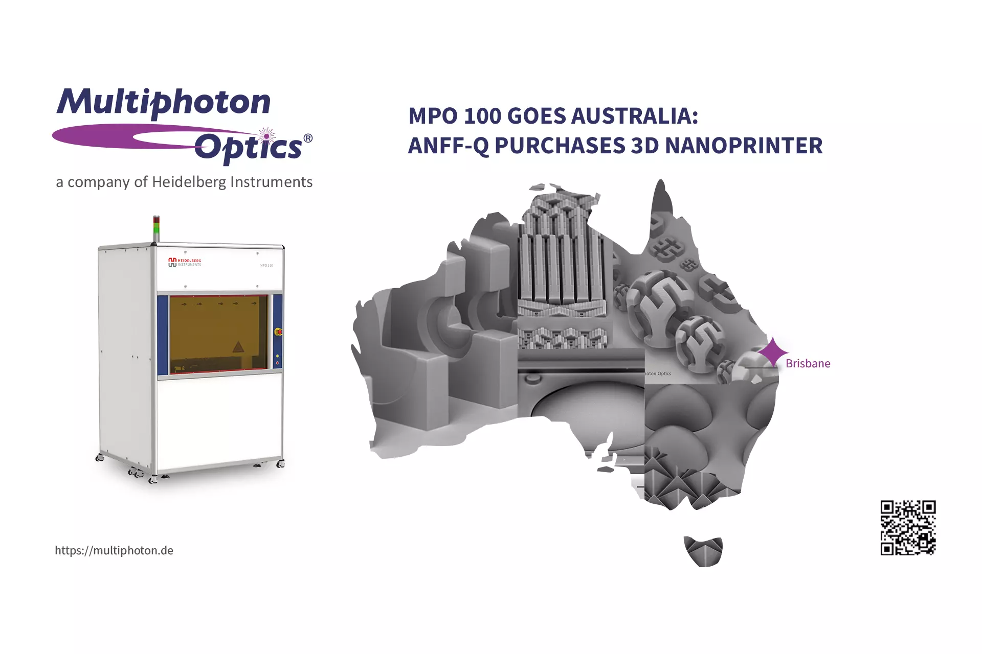
MPO 100 goes Australia: ANFF-Qld purchases 3D nanoprinter
Würzburg, Germany / Brisbane, Australia – The Australian National Fabrication Facility – Queensland Node (ANFF-Qld) based at the University of Queensland, Australia has placed a
Würzburg, Germany / Brisbane, Australia – The Australian National Fabrication Facility – Queensland Node (ANFF-Qld) based at the University of Queensland, Australia has placed a

Heidelberg, March 30, 2022. Heidelberg Instruments has received a significant order from a leading semiconductor wafer-level packaging production company in Asia for its MLA 300

Heidelberg/Würzburg, January 18, 2022. “1 – 10 – 100 – 1000” – Achievable component heights of over 1 cm, surfaces with roughness in the order

Our Applications & Service team at Heidelberg Instruments Nano recently installed the first NanoFrazor Scholar directly integrated into a custom-made Glovebox system with controlled inert

Following several very successful and happy years at our previous office in the Technopark Zurich, our team at Heidelberg Instruments Nano is delighted to announce

In the last weeks, another NanoFrazor system from Heidelberg Instruments was installed in Canada at the University of Alberta/NRC, where it will be used for fabricating

We celebrate the National Nanotechnology Day (USA) on October 9th, which pays homage to the nanometer scale: 1 nm equals 1 x 10⁻⁹ m (one

NanoFrazor Explore installation at Queen Mary University of London (Photo by Jonas Vergés) Two more NanoFrazor systems were installed in England at Queen Mary University

Heidelberg Instruments receives ISO 9001:2015 Certificate for extraordinary Quality Management Heidelberg, September 22, 2021. TÜV Süd, an auditor and provider of safety, security and sustainability

Heidelberg, Germany, 26 August 2021: Heidelberg Instruments announced order for an ULTRA Semiconductor Laser Mask Writer from a large photomask production group in China. ULTRA
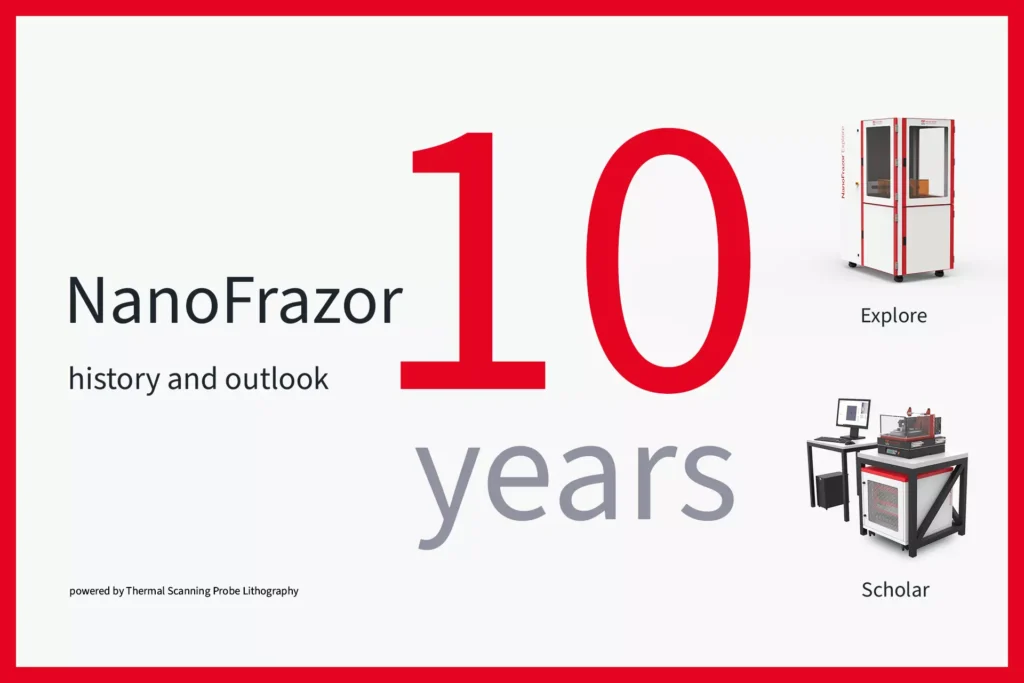
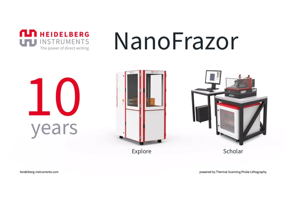
The commercialization of the NanoFrazor started in 2012. This article looks back at where the NanoFrazor came from, how it
Zurich, Switzerland / Heidelberg, Germany – Heidelberg Instruments Nano AG in Zurich, a subsidiary office of Heidelberg Instruments Mikrotechnik GmbH

Würzburg, Germany / Brisbane, Australia – The Australian National Fabrication Facility – Queensland Node (ANFF-Qld) based at the University of

Join our expert Dr. Jana Chaaban in this webinar to discover more about the working principle of the NanoFrazor lithography.

Heidelberg Instruments at the LASER World of PHOTONICS is all about the Power of Direct Writing After almost three years,
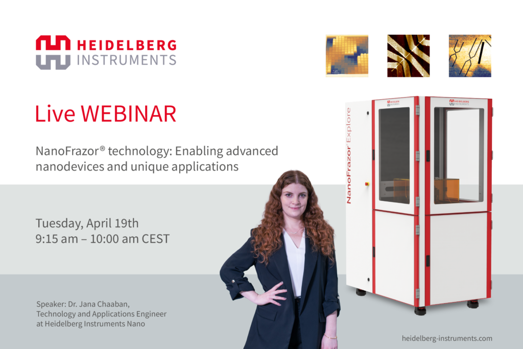
NanoFrazor technology: Enabling advanced nanodevices and unique applications register now The NanoFrazor uses thermal scanning probe lithography (t-SPL) for the

Heidelberg, March 30, 2022. Heidelberg Instruments has received a significant order from a leading semiconductor wafer-level packaging production company in
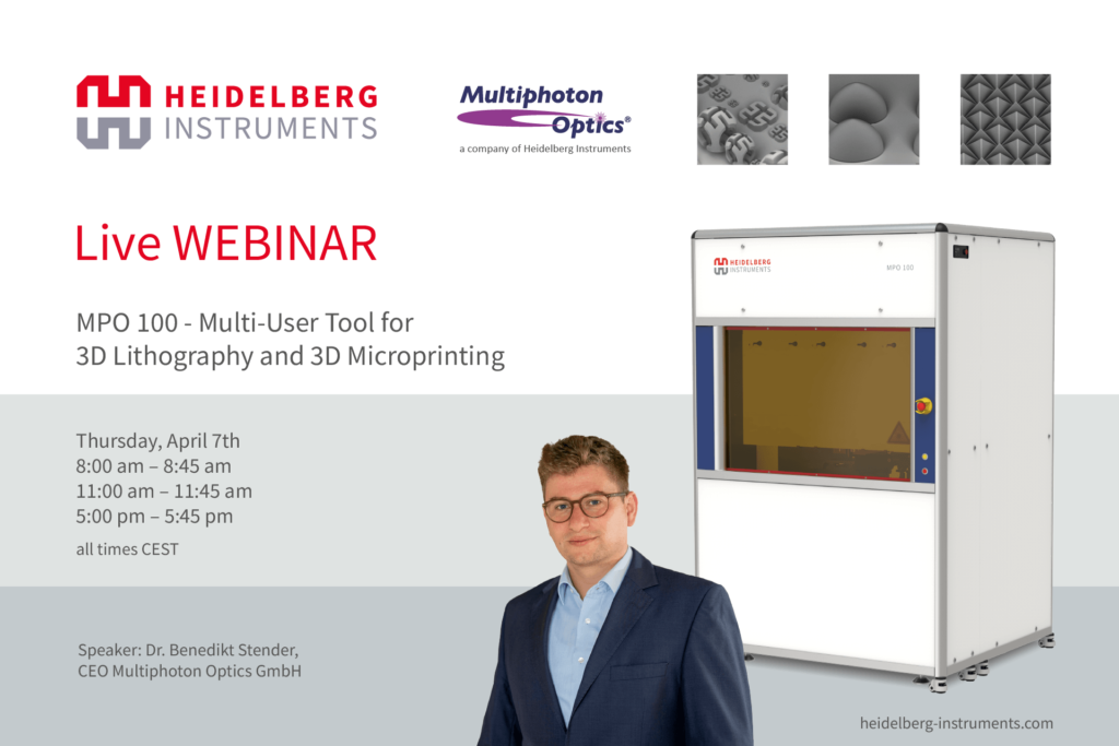
MPO 100 – Multi-User Tool for 3D Lithography and 3D Microprinting „1 – 10 – 100 – 1000” – Achievable
EPIC Virtual Company Tour at Heidelberg Instruments and Multiphoton Optics The European Photonics Industry Consortium (EPIC), Multiphoton Optics and Heidelberg

The SPIE Photonics West, the leading global conference in San Francisco, brings together experts in industrial lasers, optoelectronics, biomedical, optics