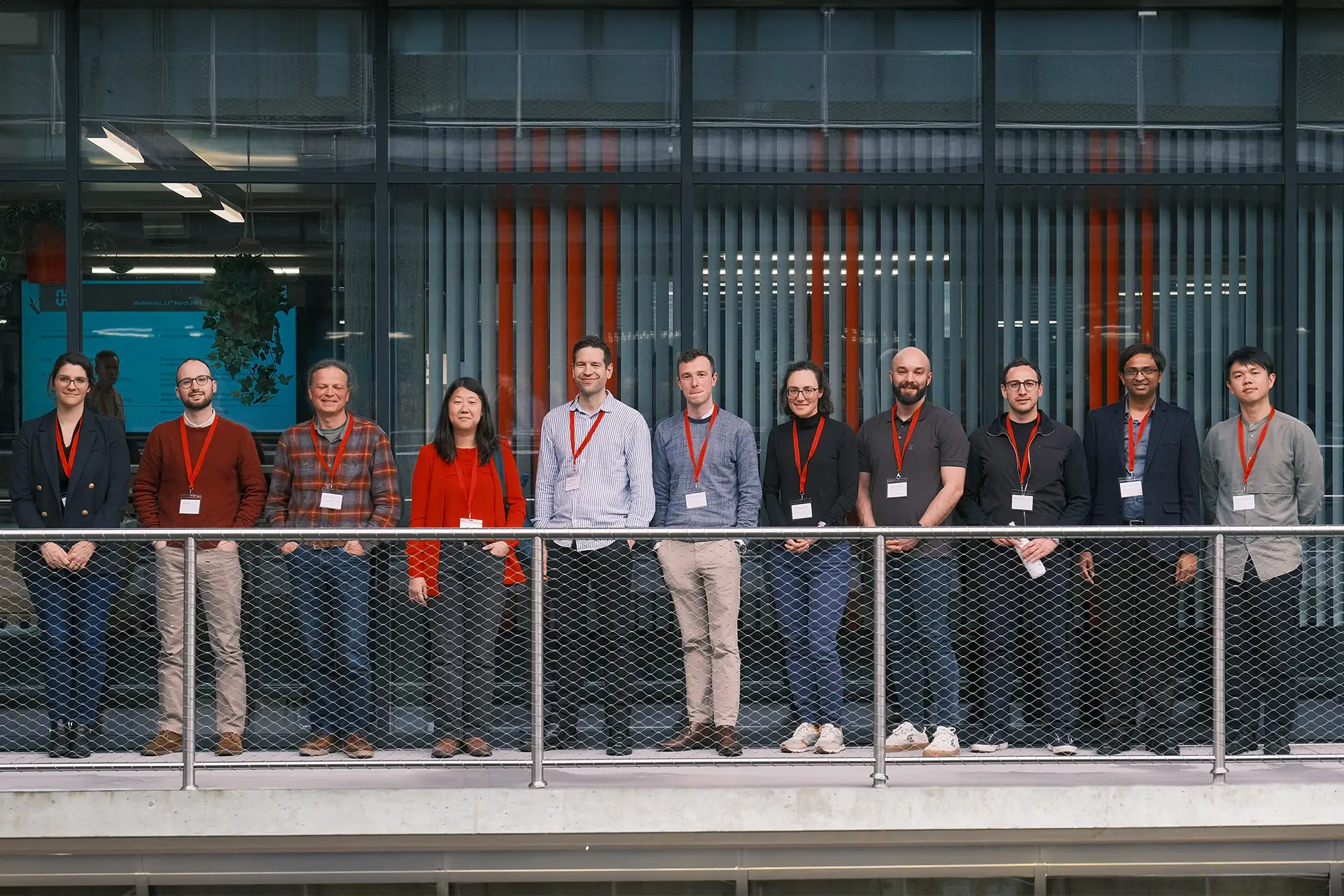
We’re happy to announce the first NanoFrazor Explore system in Latin America installed at UNICAMP, Campinas (Brazil) in the Center for Semiconductor Components (CCS).
Samuel Bisig from Heidelberg Instruments Nano performed the installation and training with the help of our local distributers QD Latin America. This is the first of many more NanoFrazor systems to come in the Latin America region.
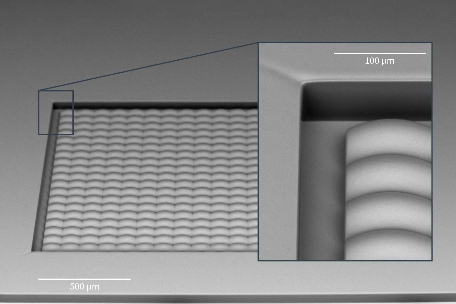
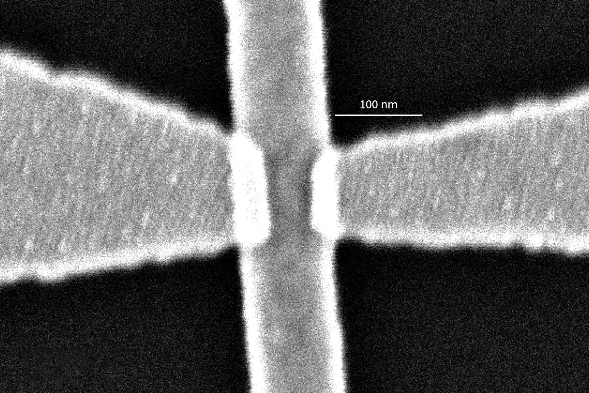
During the few days of installation and user training, Prof. Stanislav Moshkalev and his research group at CCS were already able to lift-off 5nm/15nm Ti/Au structures with minimum feature sizes <100nm. They plan to use the NanoFrazor further across multiple research groups for applications in nanoelectronics, nanophotonics, microelectronics and beyond.
We wish our newest NanoFrazor users all the best in their research and know that our tool’s capabilities will even spark new ideas and applications!