Overview on Maskless Grayscale Lithography
From design to micro structured topography: Grayscale lithography can be used to quickly fabricate various 2.5D and 3D structures at the micro scale.
From design to micro structured topography: Grayscale lithography can be used to quickly fabricate various 2.5D and 3D structures at the micro scale.
Grayscale lithography can create structured surfaces in photoresist for micro-optics applications. Experiments show promise in fabricating structures over 100 μm using a new experimental resist.
Utilizing grayscale lithography and hard-mask methods, silicon carbide hosts micrometer-scale features and hemispherical solid immersion lenses, boosting optical collection for quantum emitters. Scalable, reproducible, CMOS-compatible.
We present the powerful software solution 3D-PEC of GenISys BEAMER for rapid and easy optimization of complex 3D microstructures fabricated with Grayscale laser lithography.
The Quantum Issue of The Lithographer, issued Fall 2020 Topics include: Maskless Aligners, Grayscale, 2D Materials, Quantum Technology
We investigate neurite guidance using semiconductor industry-compatible techniques for fabricating modulated surfaces, enabling the cultivation and study of ordered neuronal networks in a 2.5D configuration.
A flat lens, designed through inverse design with a phase-only pupil function, achieves achromatic focusing over a broad spectrum in a single diffractive surface.
Inverse design enables the creation of thin, high-NA flat lenses. Multi-level diffractive lens (MDL) with a NA=0.9 at 850 nm wavelength, replicable via imprint lithography.
The Rise of Grayscale Lithography: Direct-write 3D patterning scaled from µm to nm. Grayscale Lithography Issue of The Lithographer, issued January 2020.
Multi-level diffractive lens (MDL) designs drastically enhance depth of focus by over 4 orders of magnitude, enabling focus maintenance for objects separated by large distances.

Exciting news! At Kyoto University Nanotechnology Hub one MPO 100 3D microprinting system and one MLA 150 maskless lithography system
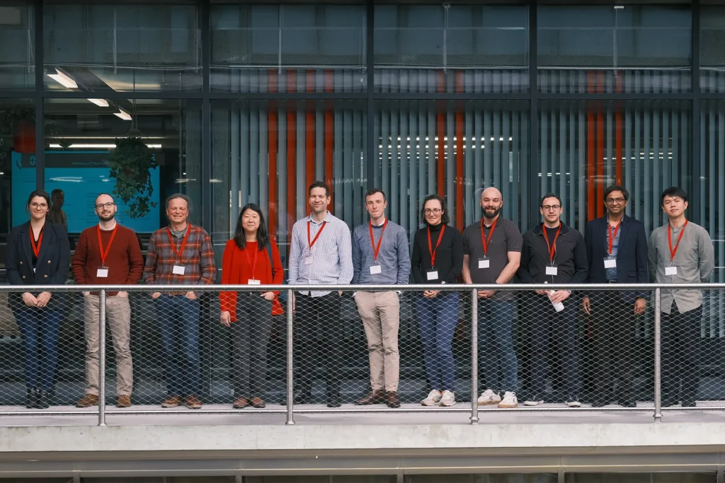
A look back on the 8th Thermal Probe Workshop We were delighted to host a community of nanotechnology experts, fabrication
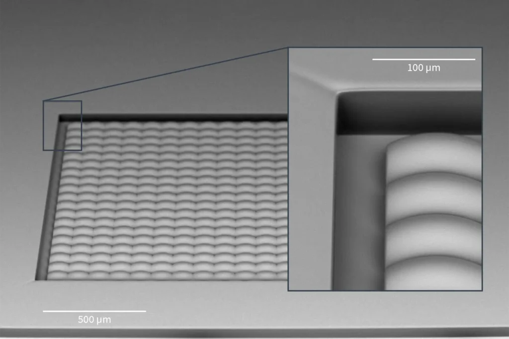
Achieve high throughput and resolution. Despite its unique capacity for three-dimensional fabrication with minimal feature sizes below 100 nm, achieving
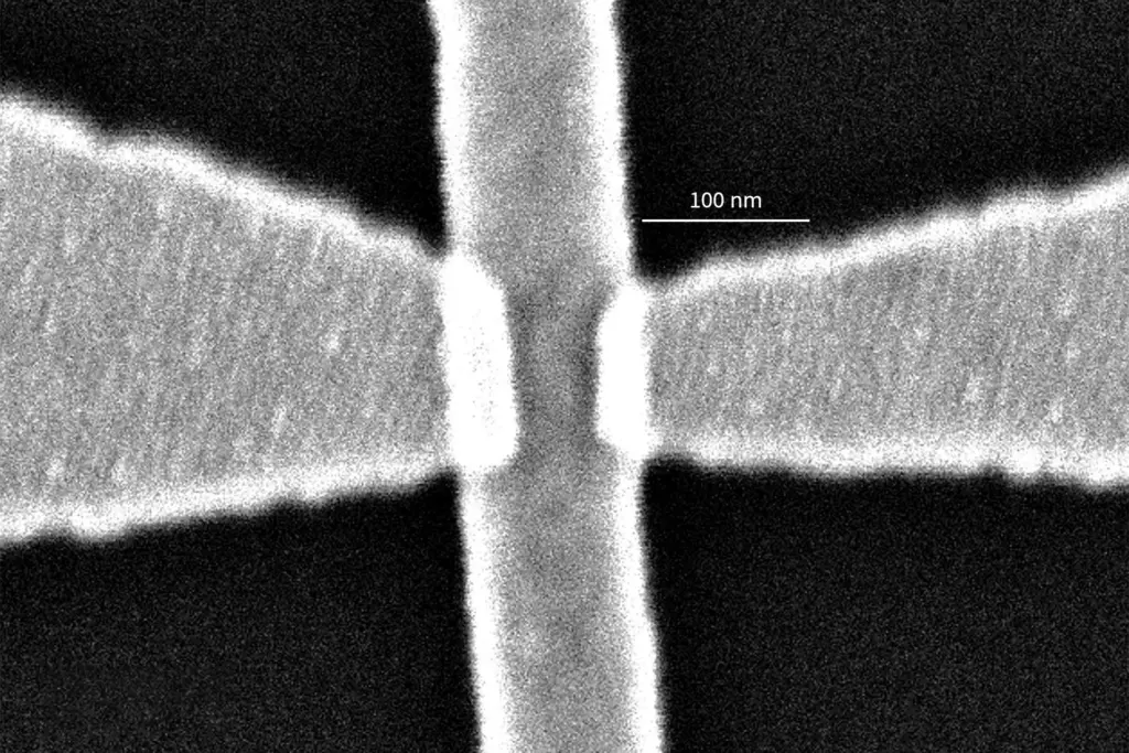
Discover our two Application Notes covering this topic: “Bilayer Lift-Off for NanoFrazor Lithography”“Ultra-High Resolution Pattern Transfer on NanoFrazor Lithography” In
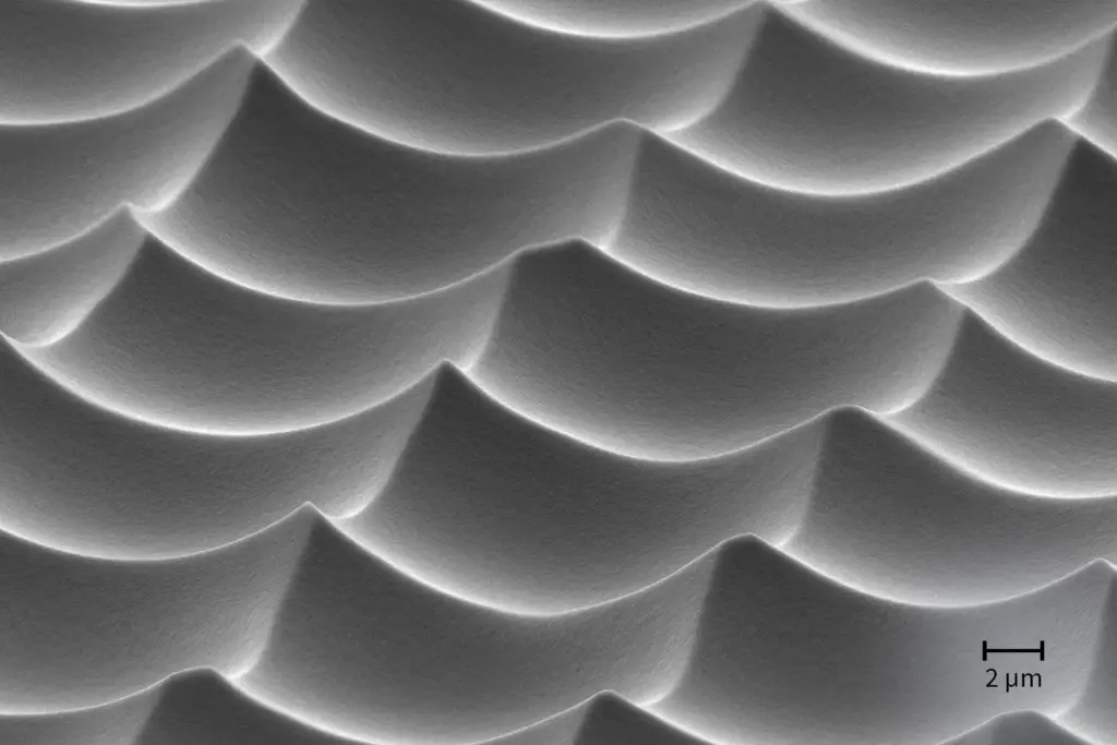
Advancing Excellence in Microfabrication: Fabrication of 2.5D Topographies with Maskless Grayscale Lithography or Two-Photon Polymerization (TPP) What looks like ocean
2024 will mark Heidelberg Instruments‘ 40th anniversary. With gratitude we look back, with joy we look forward to what’s ahead.

Season’s Greetings from Heidelberg Instruments! In the spirit of joy and gratitude, we extend our warmest wishes to our valued
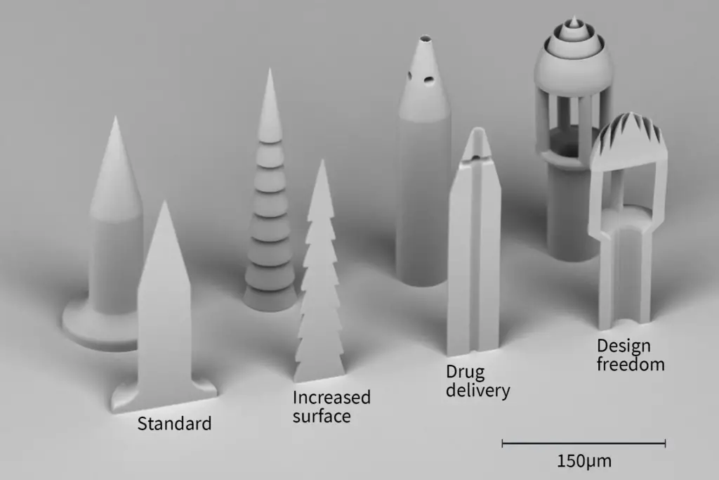
Microneedles as alternative to conventional drug administration Commonly used methods of drug delivery are associated with certain drawbacks: As an
The Heidelberg Instruments booth at SEMICON EUROPA 2023 in Munich from November 14th -17th attracted a wide range of visitors
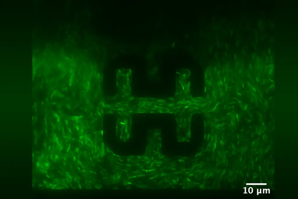
The EIPBN conference, which stands for the International Conference on Electron, Ion, and Photon Beam Technology and Nanofabrication, and is
We are always at your disposal.
Please send us your request.
To view the form, please enable Marketing cookies.
Subscribe to our newsletter
to receive the newest information.
To view the form, please enable Marketing cookies.