Light-induced anomalous Hall effect in graphene
Optical driving in quantum solids uncovers phenomena like light-induced superconductivity and anomalous Hall effect in graphene, revealing Floquet-engineered topological band structures.
Multi-level diffractive lens (MDL) designs drastically enhance depth of focus by over 4 orders of magnitude, enabling focus maintenance for objects separated by large distances.
With the control of the phase in the image plane, a single diffractive surface can correct chromatic aberrations over a wide bandwidth, simplifying imaging systems.
Two-photon absorption (TPA) provides freedom in design for the fabrication of novel products that are not feasible with conventional techniques.
Thermal Scanning Probe Lithography enables precise metal electrode patterning on 2D semiconductors like MoS2, improving device performance with vanishing Schottky barriers and exceptional properties.
Creating precise nanofluidic slits, utilizing electrostatic forces and oscillating fields, enables controlled transport of nanoparticles, demonstrated with 60nm gold spheres and efficient sorting of particles.
Achromatic diffractive lenses (ADLs) enable imaging across the visible spectrum, achieving diffraction-limited focusing and high numerical aperture. Cost-effective and scalable for widespread use.
Via-hole oxidation process for forming buried oxide-confined waveguides, resulting in straight, low-loss waveguides with smooth interfaces, simplifying III-V-semiconductor-oxide photonic device fabrication.
First experimental demonstration of vertically-coupled micro-disk resonators to buried access waveguides on III-V semiconductor using simplified three-dimensional integration scheme, achieving high-quality devices.
Bottom surface-induced ferromagnetism in Bi2Se3 nanoplate devices on SiO2 and ferromagnetic insulator substrates decouples quantum Hall effects, revealing shifted half-integer QHEs in a three-channel model.
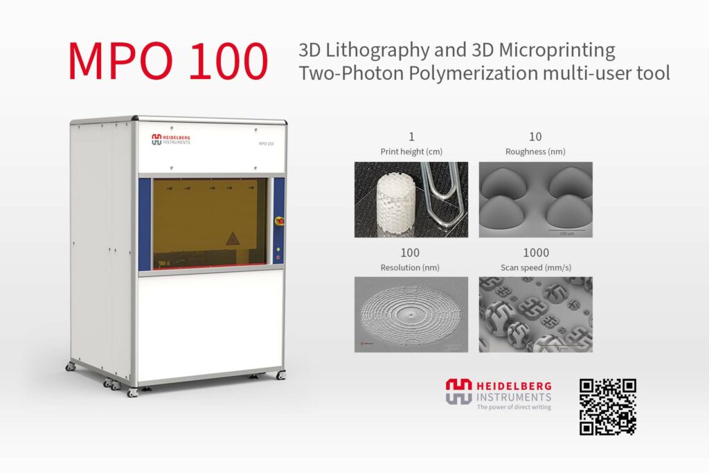
Heidelberg/Würzburg, January 18, 2022. “1 – 10 – 100 – 1000” – Achievable component heights of over 1 cm, surfaces
We rely heavily on electronics for virtually everything we do. But actually, it does not necessarily need to be electrons
Our best wishes for a healthy, prosperous New Year Thank you very much for your confidence and your co-operation in
Our Applications & Service team at Heidelberg Instruments Nano recently installed the first NanoFrazor Scholar directly integrated into a custom-made
Following several very successful and happy years at our previous office in the Technopark Zurich, our team at Heidelberg Instruments
Scanning Tunnelling Microscopy (STM) relies on quantum tunnelling for imaging and manipulation of objects on atomic scale. It is one
International, innovative, unrivaled: productronica has always been the largest international event for the electronics production industry and the only trade
Quantum computers are one of the most exciting developments of today’s physics. There are a lot of open questions in
Research in many fields of modern physics requires micro- or nanoscale devices. Nanofabrication has achieved a truly amazing level of
High-resolution lithography has played a central role in the nanotechnology revolution of the past decade. While ultra-high resolution lithography (<50
We are always at your disposal.
Please send us your request.
To view the form, please enable Marketing cookies.
Subscribe to our newsletter
to receive the newest information.
To view the form, please enable Marketing cookies.