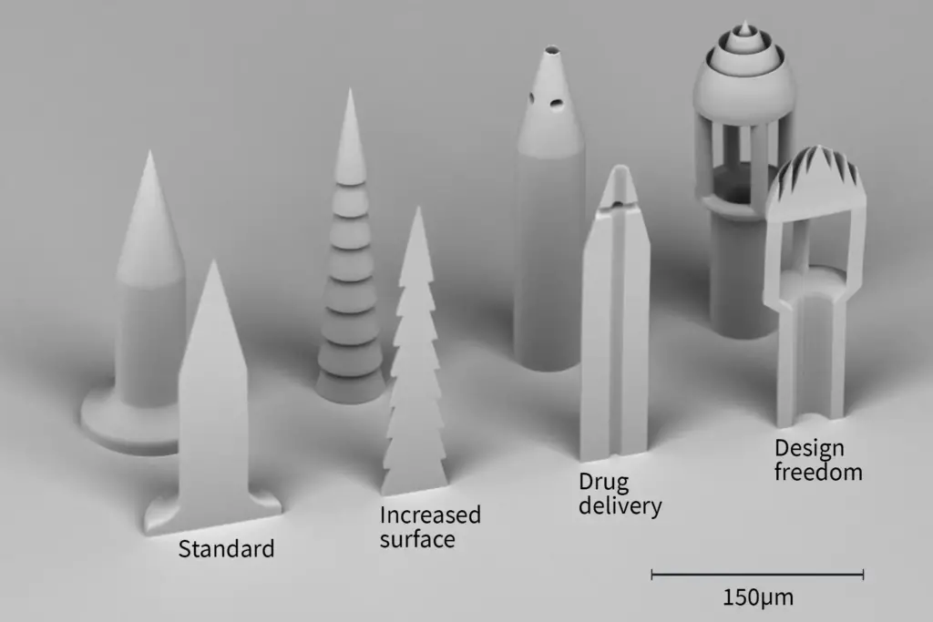
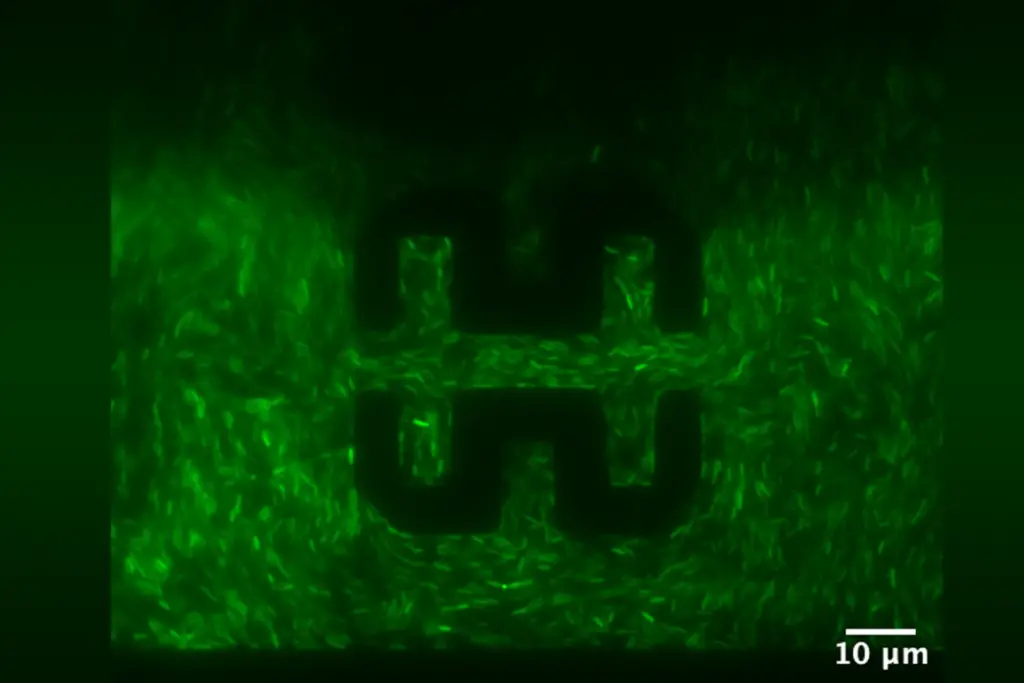
Biosynthesis enhancement of tropodithietic acid (TDA) antibacterial compound through biofilm formation by marine bacteria Phaeobacter inhibens on micro-structured polymer surfaces
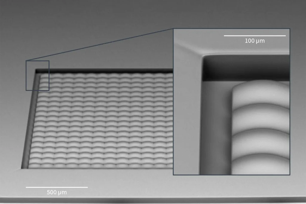
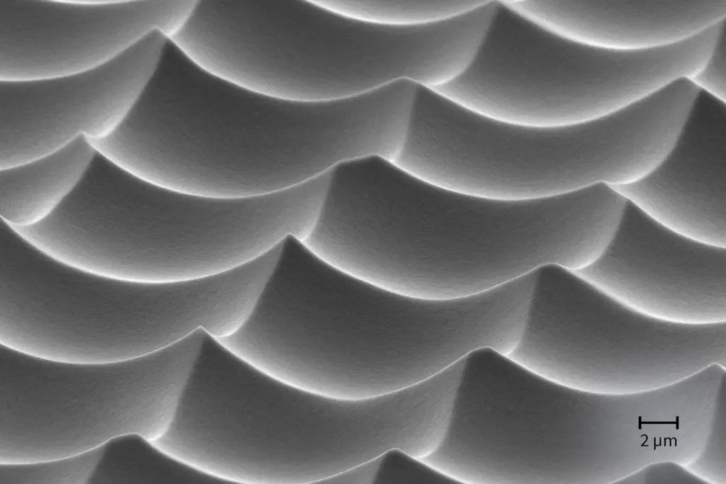
Microfluidic channels cultivate Phaeobacter inhibens biofilms on diverse polymer surfaces, offering biocontrol potential in aquaculture by mitigating antibiotic risks. Creating diverse surfaces to promote biosynthesis.