Microfluidics and nanofluidics are rapidly growing fields that involve manipulating small volumes of fluids in channels with micrometer and nanometer dimensions, respectively. These technologies find extensive applications in chemical and biological research, medical diagnostics, and industrial settings and enable the development of lab-on-a-chip devices, offering miniaturized platforms for chemical and biological reactions.
These devices provide advantages like reduced sample volumes, faster reaction times, and enhanced sensitivity, making them valuable in drug discovery, point-of-care diagnostics, and environmental monitoring. Microfluidic devices can feature various structures, and fabrication materials include SU-8 and mr-DWL resists, patterned using direct-write lithography tools like DWL and MLA series. For complex 3D structures, the MPO 100 utilizes two-photon polymerization.
On the other hand, nanofluidics is crucial in nano- and biotechnology applications, where precise handling of tiny liquid volumes is necessary. It encompasses DNA sequencing, sorting, assembling, and manipulating nanoparticles, proteins, enzymes, and viruses. Nanofluidic structures demand excellent shape control, and various materials, including biocompatible polymers and epoxies, can be used. The NanoFrazor employs grayscale patterning capabilities, enabling efficient creation of nanofluidic systems. Its closed-loop lithography approach and integrated topography sensor ensure high accuracy and ultrahigh resolution, making it advantageous for nanofluidics applications. As technology advances, microfluidics and nanofluidics are set to play increasingly vital roles in various fields, from basic research to medical diagnostics.
Used to pattern either simple or complex 2.5D topographies (e.g., tapered channels)
3D microstructures (MPO 100)
High aspect ratio
Tall channels with vertical side walls (MLA series)
No undercut
The structure can be used for replication
Nanoscale thermal conversion (NanoFrazor)
E.g., local binding of amine groups
Microfluidics and nanofluidics are rapidly growing fields that involve manipulating small volumes of fluids in channels with micrometer and nanometer dimensions, respectively. These technologies find extensive applications in chemical and biological research, medical diagnostics, and industrial settings and enable the development of lab-on-a-chip devices, offering miniaturized platforms for chemical and biological reactions.
These devices provide advantages like reduced sample volumes, faster reaction times, and enhanced sensitivity, making them valuable in drug discovery, point-of-care diagnostics, and environmental monitoring. Microfluidic devices can feature various structures, and fabrication materials include SU-8 and mr-DWL resists, patterned using direct-write lithography tools like DWL and MLA series. For complex 3D structures, the MPO 100 utilizes two-photon polymerization.
On the other hand, nanofluidics is crucial in nano- and biotechnology applications, where precise handling of tiny liquid volumes is necessary. It encompasses DNA sequencing, sorting, assembling, and manipulating nanoparticles, proteins, enzymes, and viruses. Nanofluidic structures demand excellent shape control, and various materials, including biocompatible polymers and epoxies, can be used. The NanoFrazor employs grayscale patterning capabilities, enabling efficient creation of nanofluidic systems. Its closed-loop lithography approach and integrated topography sensor ensure high accuracy and ultrahigh resolution, making it advantageous for nanofluidics applications. As technology advances, microfluidics and nanofluidics are set to play increasingly vital roles in various fields, from basic research to medical diagnostics.
Smooth surface
High aspect ratio structures
Ultra-high-resolution holes and channels
Accurate grayscale lithography for channels (particles guiding)
High resolution (DWL & MLA series) and ultra-high resolution (NanoFrazor)
Used to pattern either simple or complex 2.5D topographies (e.g., tapered channels)
3D microstructures (MPO 100)
High aspect ratio
Tall channels with vertical side walls (MLA series)
No undercut
The structure can be used for replication
Nanoscale thermal conversion (NanoFrazor)
E.g., local binding of amine groups
Application images
Microfluidic chip made of SU-8
Microfluidic chip made of SU-8, meandering channel, width 200 µm
Microfluidic chip made of SU-8, mixer, pillar diameter 150 µm
Microfluidic chip made of SU-8, mixer, pillar diameter 150 µm
Microfluidic chip made of SU-8, waste reservoir, channel width 150 µm
Microfluidics channels in 25 µm of SU-8 fabricated by Maskless Lithography.
The image shows a master of a microfluidic mixer in 100 μm SU-8, which can be patterned with the 375 nm wavelength option of the MLA 150. This type of structure is typically transferred by soft lithography in PDMS. (Courtesy of CMi EPFL Center of MicroNanoTechnology)
MPO 100: Capable of fabricating microfluidic structures with high complexity.
The nanostructure of a tendon tissue (left: AFM of the original tendon) patterned and imaged with NanoFrazor Explore into biocompatible PPA resist (right image).
(Courtesy of Melbourne Nanofabrication Center, published in 2019)
Nanofluidic ratchets fabricated with single-nanometer accuracy by NanoFrazor patterning.
(Courtesy of IBM Research, Publications in Science and PRL 2018)
Thermolysin enzymes trapped in 10-nm-wide lines written with a NanoFrazor Explore.
(Courtesy of Riedo group at NYU, Publications in 2019)
suitable Systems
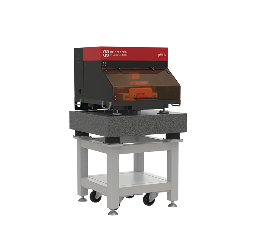
µMLA
Maskless Aligner
Configurable and compact tabletop maskless aligner with raster scan and vector exposure modules.
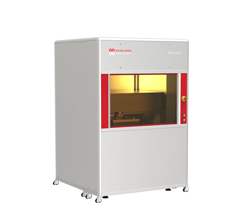
MLA 150
Maskless Aligner
The fastest maskless tool for rapid prototyping, the alternative to the mask aligners. Perfect for standard binary lithography.
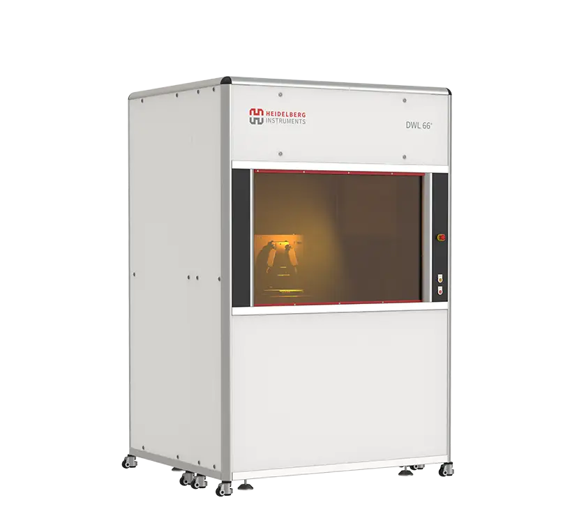
DWL 66+
Direct Write Laser Lithography System
Our most versatile system for research and prototyping with variable resolution and wide selection of options.
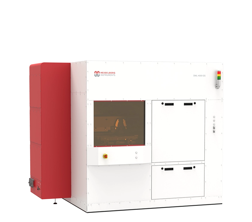
DWL 2000 GS / DWL 4000 GS
Direct Write Laser Lithography System
The most advanced industrial grayscale lithography tool on the market.
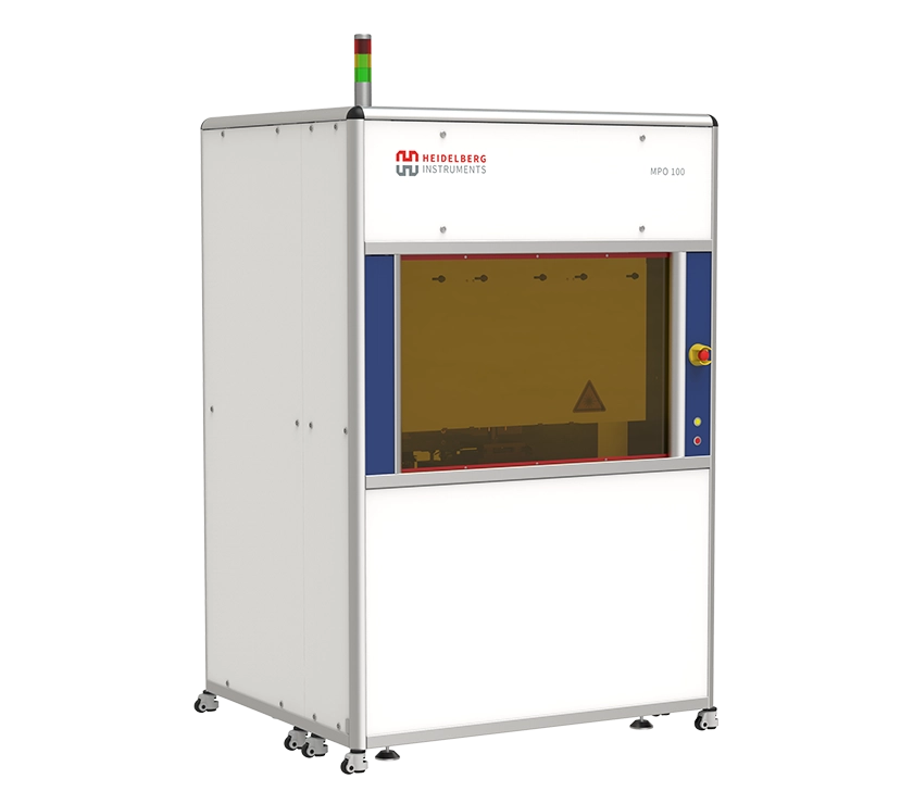
MPO 100
Two-Photon Polymerization Multi-User Tool
Multi-User Tool for 3D Lithography and 3D Microprinting of microstructures with applications in micro-optics, photonics, micro-mechanics and biomedical engineering.
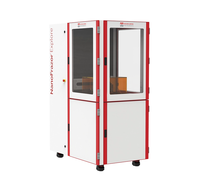
NanoFrazor Explore
Thermal Scanning Probe Lithography System
Thermal scanning probe lithography tool with direct laser sublimation and grayscale modules. Excellent alternative to e-beam lithography tools.