Newsblog

Application Note: Ultra-High Resolution Pattern Transfer

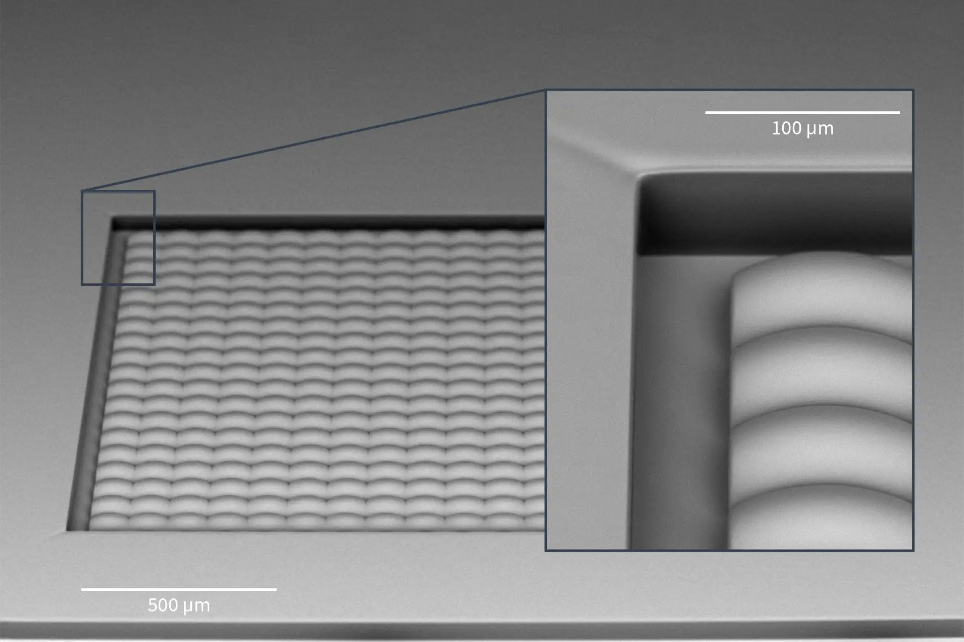
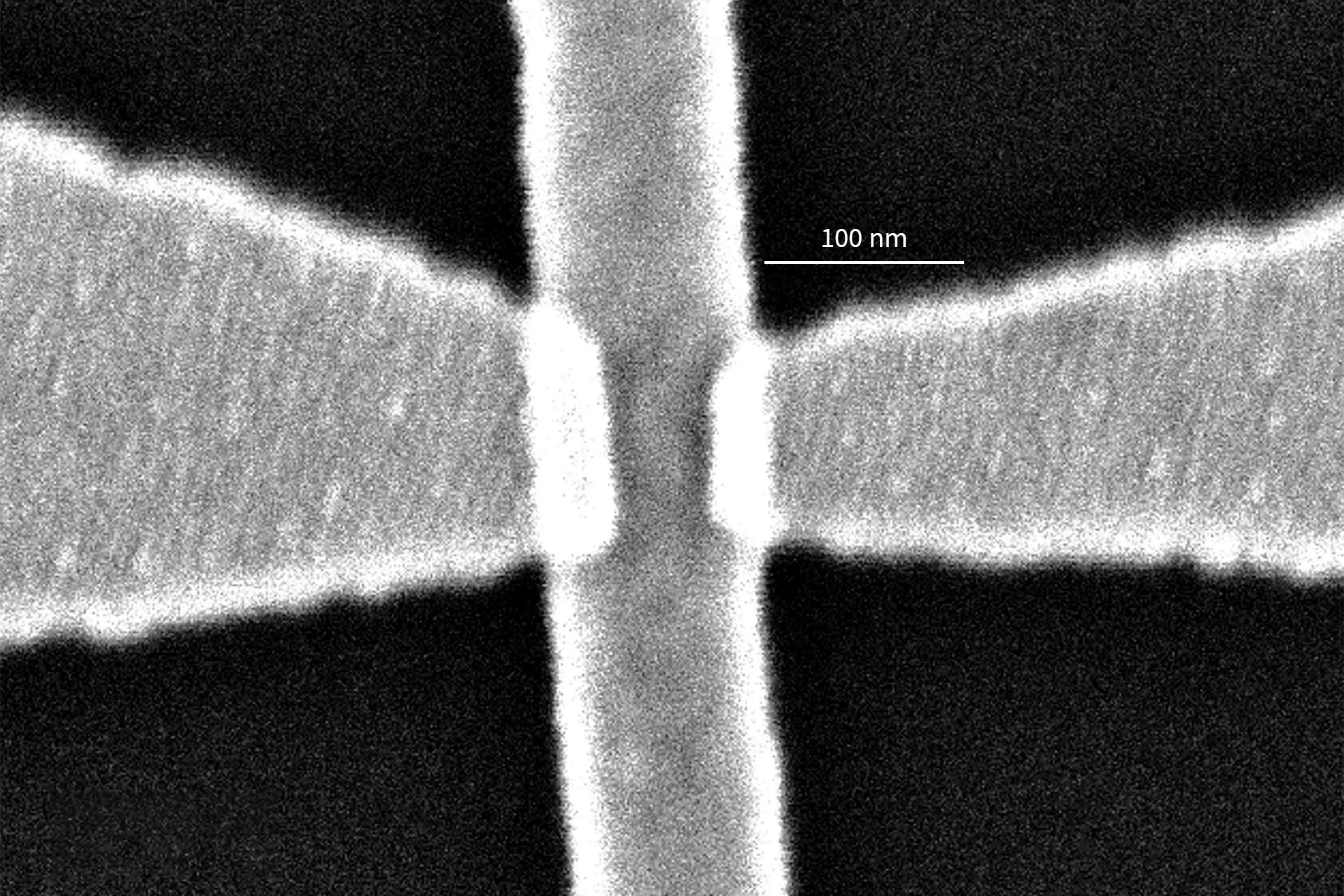
High-resolution lithography has played a central role in the nanotechnology revolution of the past decade. While ultra-high resolution lithography (<50 nm) is the focus of many research and industrial efforts, pattern transfer – the subsequent step to lithography – presents many challenges of its own.

This application note shows how we can combine the capabilities of the NanoFrazor lithography with especially customized etching and lift-off methods for the successful transfer of ultra-high resolution patterns.

Read this application note in our

To access this document type in “pattern transfer” into the search bar or filter for the category “Application Note” and for the tag “NanoFrazor”

Share:

Related Posts

Maskless lithography provides the extreme overlay accuracy which is central to applications in the sensor field: The production of SQUID devices may involve as many as 18 layers and high-resolution features. The alignment between layers is crucial to the production yield and is completed automatically with the Maskless Aligner technology (impressively demonstrated here by the MLA 150).

Beyond Theory: Engineering Quantum Devices with Precision Lithography

The quantum revolution is shifting from theory to reality, as breakthroughs like Google’s “Quantum Echoes” show. Scaling from small demos to systems with thousands of qubits demands ultra-precise, uniform nanofabrication. This post examines the fabrication challenges and lithographic solutions enabling the leap from lab to large-scale production.

Scroll to Top