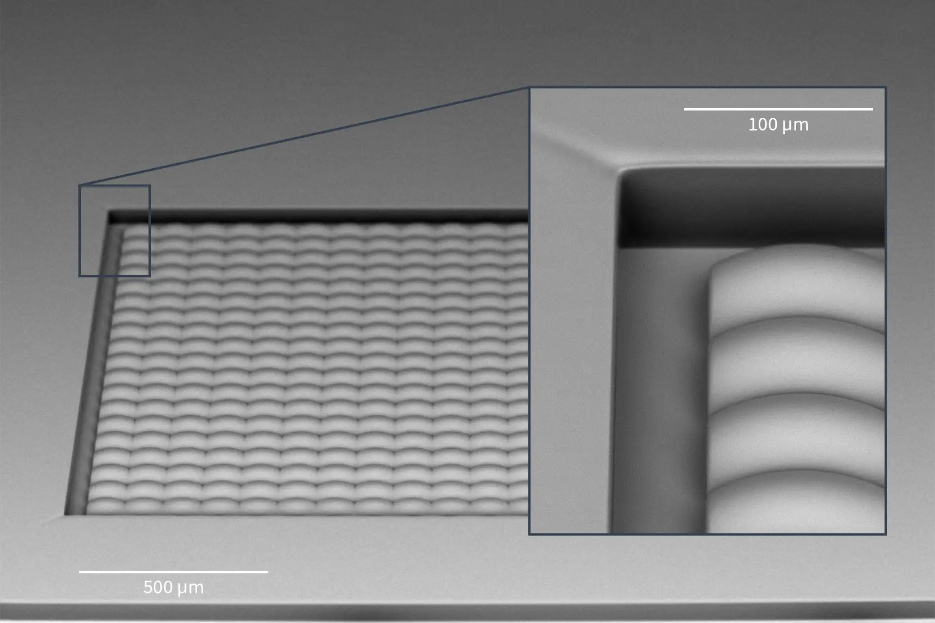
Thermal scanning probe lithography (t-SPL), enabled by NanoFrazor, uses a heatable ultrasharp
tip for simultaneous patterning and inspection of nanostructures in thermal resists.
Thanks to its non-invasive patterning principle, namely the lack of charged particles, the
NanoFrazor technology allows for the fabrication of novel nanodevices with material systems
and architectures that would otherwise not be possible with alternative nanolithography
techniques.
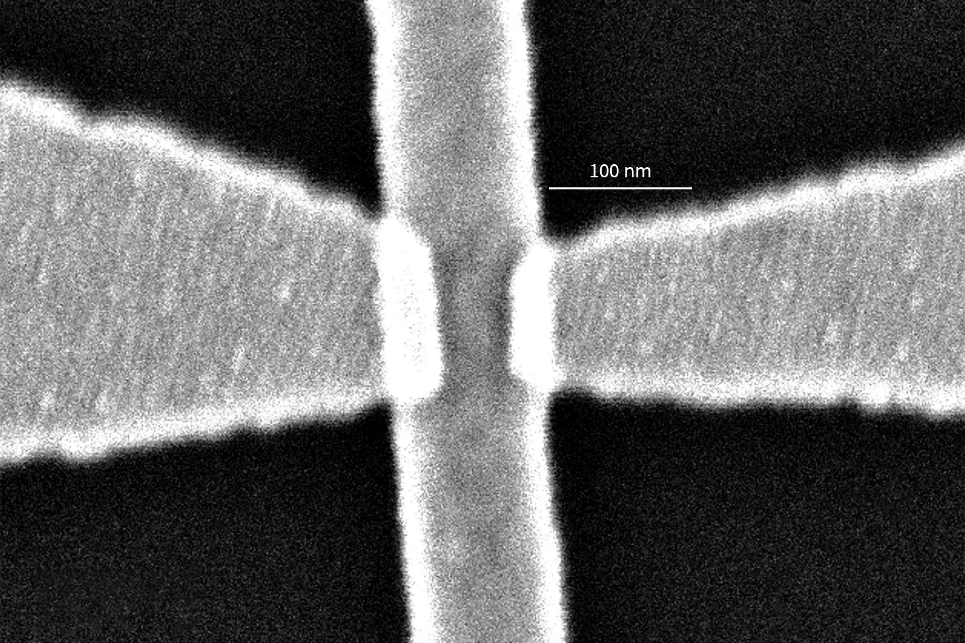
The NanoFrazor technology has also proven its value as an asset for improving the performance of existing device concepts.
In this application note, we discuss two examples of
NanoFrazor-fabricated devices, nanowire-based field effect transistors (FETs) and 2D-material
transistors, and highlight their superior performance as compared to their counterpart made by
charged particle-based nanolithography methods.