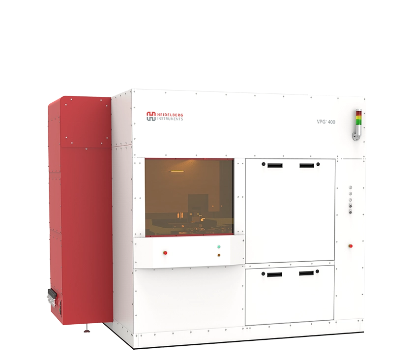
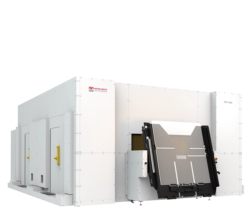
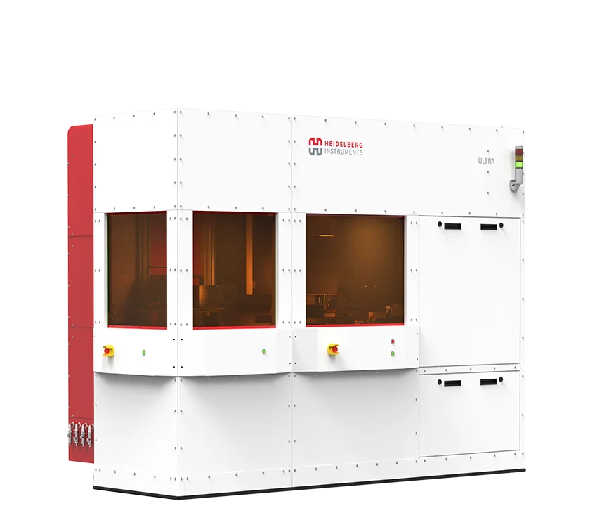
Traditional photolithography requires the fabrication or purchase of a photomask and then the use of a stepper or mask aligner to transfer the CAD pattern onto a resist-covered wafer or plate. This process is the most established and feasible method for high-volume manufacturing of sub-micron sized design features. In fact, Heidelberg Instruments offers systems such as the VPG+ series or ULTRA that are specifically designed for the photomask market, from mature semiconductor photomasks, to electronics and FPD photomasks.
There is, however, another photolithography technique available which constitutes a perfect alternative for many other applications: Maskless Lithography. This state-of-the-art, high-precision, highly flexible technology is ideal for use in both R&D as well as environments where rapid-prototyping of feature sizes greater than 1 µm are required. The maskless lithography technique allows you to bypass the long process of ordering a photomask and enables you to transfer the design directly to the wafer without the need for a photomask.
In maskless lithography the pattern is exposed directly onto the substrate surface with the help of a spatial light modulator, or SLM, which serves as a “dynamic photomask”. Simply upload and convert the design file and the maskless aligner will take care of the rest. As your pattern evolves, simply reload the design and do as many exposures as is necessary over a much shorter period of time than what is possible with a traditional mask-based technique.
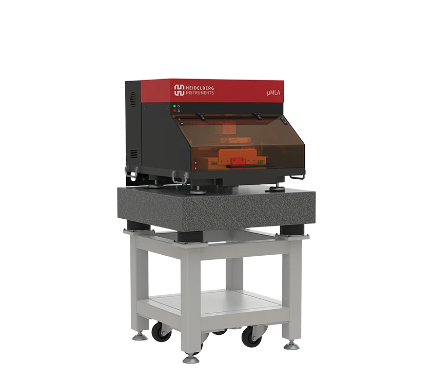
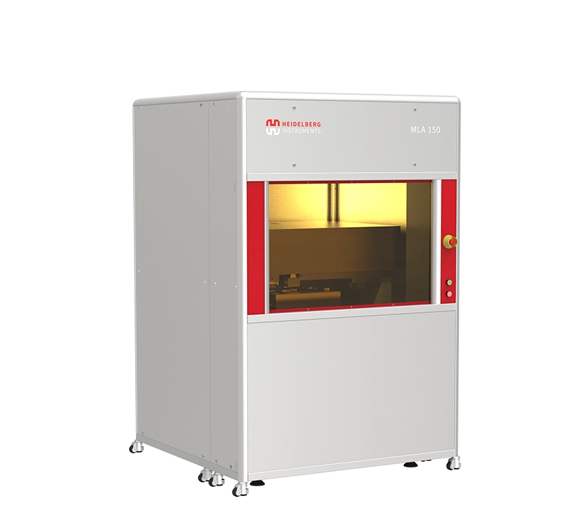
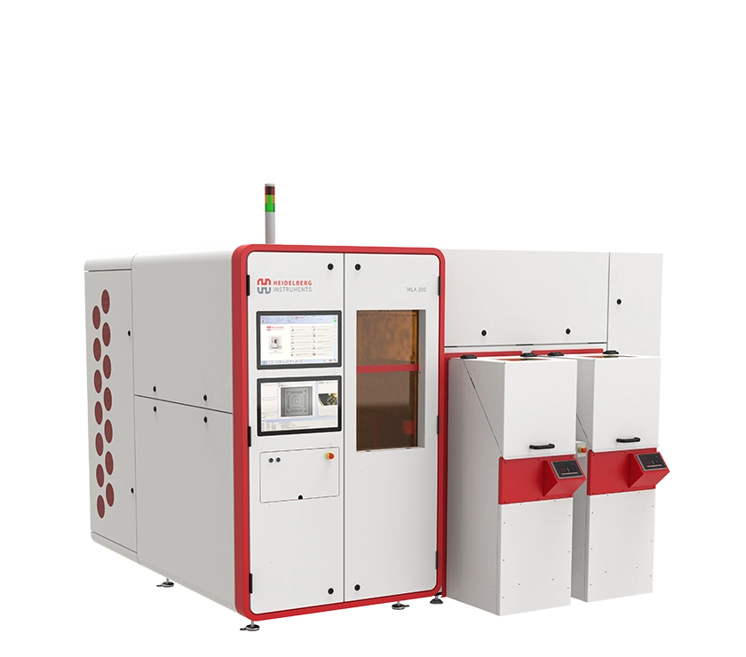
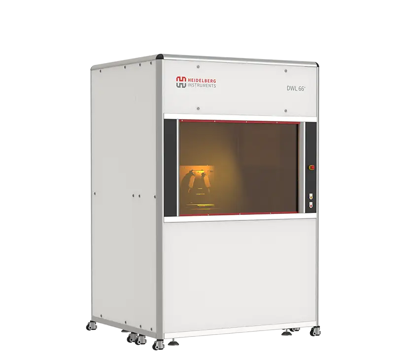
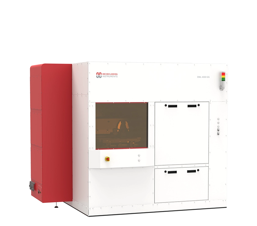
Discover our Maskless Aligners (MLA) and Direct Write Lithography (DWL) optical lithography systems.