1D & 2D Materials
Low-Damage Lithography with High-Accuracy Overlay on Sensitive 1D & 2D Materials
-
Description
-
Devices made using one-dimensional (1D) and two-dimensional (2D) structures can exhibit fascinating physical phenomena, unlocking potential applications in high-performance electronics, sensing, and quantum computing, as well as photonic devices for use in communications and energy harvesting. They also have potential uses in ultra-strong and lightweight materials for aerospace and automotive industries, flexible and transparent electronics for wearable technology and displays, and energy storage and water purification. However, impurities and defects can significantly limit the performance of these devices.
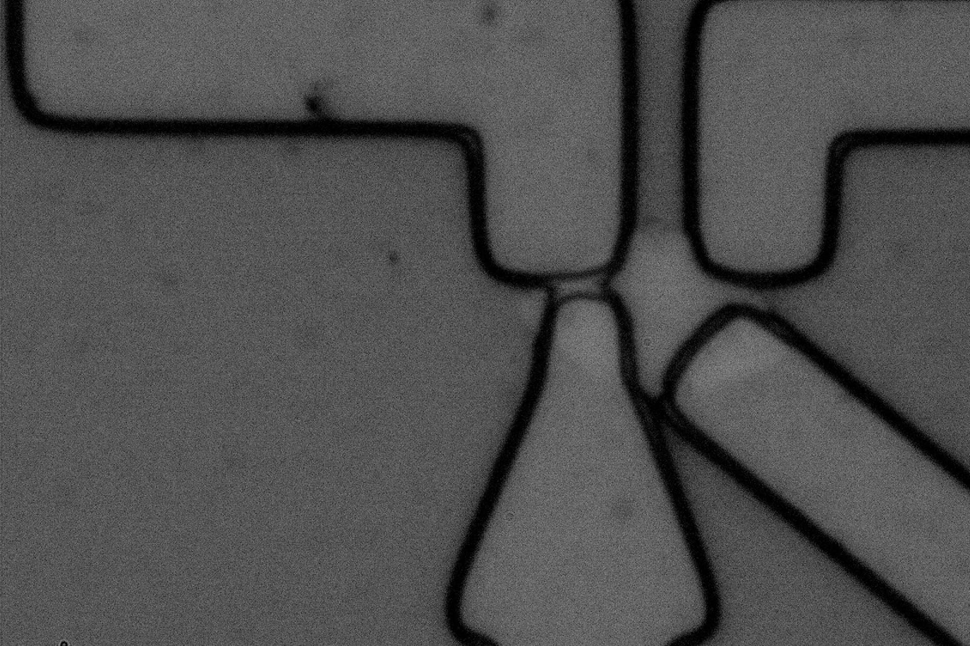
To overcome this challenge, Heidelberg Instruments provides tools that can pattern 1D or 2D materials with precision and accuracy, while avoiding impurities and defects. For example, the NanoFrazor provides a damage-free lithography solution for such applications, without charging effects or energetic beams impinging on the material surfaces. Accurate overlay on the nanostructures of interest is carried out directly in the NanoFrazor software, taking advantage of the integrated topography sensor combined with automation-ready workflows. The NanoFrazor systems have in-situ imaging capabilities similar to AFM, enabling accurate alignment of ultra-high resolution patterns with small elements such as wires, ribbons, tubes, or flakes, thereby reducing the likelihood of introducing impurities or defects. Heidelberg Instruments also provides dedicated post-processing recipes for device fabrication to complement the nanolithography with overlay.
In addition, the MLA series maskless aligners have a “Draw Mode” that enables the creation of an overlaying design on top of a real-time microscope image of small elements, making it ideal for creating connections while also preventing impurities and defects.
With the help of these tools, devices made from 1D and 2D materials can have improved performance and can be utilized in a wide range of applications.
-
Requirements
-
Preserve and keep pristine the material’s properties
Highly accurate and fast alignment (e.g., to flakes or existing electrodes)
High resolution patterning capabilities (e.g., for creation of ribbons)
Inert atmosphere for 2D materials sensitive to contact with air
-
Solutions
-
Markerless overlay
In-situ AFM for high-accuracy alignmentNon-invasive patterning
Material properties not affected by charged particles or resist residuesUltra-high resolution (NanoFrazor)
Narrow gaps, ribbons, gate electrodes, constrictions, etc.Glovebox (NanoFrazor & µMLA)
Nano-patterning of sensitive materials in a controlled inert atmosphere
Devices made using one-dimensional (1D) and two-dimensional (2D) structures can exhibit fascinating physical phenomena, unlocking potential applications in high-performance electronics, sensing, and quantum computing, as well as photonic devices for use in communications and energy harvesting. They also have potential uses in ultra-strong and lightweight materials for aerospace and automotive industries, flexible and transparent electronics for wearable technology and displays, and energy storage and water purification. However, impurities and defects can significantly limit the performance of these devices.
To overcome this challenge, Heidelberg Instruments provides tools that can pattern 1D or 2D materials with precision and accuracy, while avoiding impurities and defects. For example, the NanoFrazor provides a damage-free lithography solution for such applications, without charging effects or energetic beams impinging on the material surfaces. Accurate overlay on the nanostructures of interest is carried out directly in the NanoFrazor software, taking advantage of the integrated topography sensor combined with automation-ready workflows. The NanoFrazor systems have in-situ imaging capabilities similar to AFM, enabling accurate alignment of ultra-high resolution patterns with small elements such as wires, ribbons, tubes, or flakes, thereby reducing the likelihood of introducing impurities or defects. Heidelberg Instruments also provides dedicated post-processing recipes for device fabrication to complement the nanolithography with overlay.
In addition, the MLA series maskless aligners have a “Draw Mode” that enables the creation of an overlaying design on top of a real-time microscope image of small elements, making it ideal for creating connections while also preventing impurities and defects.
With the help of these tools, devices made from 1D and 2D materials can have improved performance and can be utilized in a wide range of applications.
Preserve and keep pristine the material’s properties
Highly accurate and fast alignment (e.g., to flakes or existing electrodes)
High resolution patterning capabilities (e.g., for creation of ribbons)
Inert atmosphere for 2D materials sensitive to contact with air
Markerless overlay
In-situ AFM for high-accuracy alignment
Non-invasive patterning
Material properties not affected by charged particles or resist residues
Ultra-high resolution (NanoFrazor)
Narrow gaps, ribbons, gate electrodes, constrictions, etc.
Glovebox (NanoFrazor & µMLA)
Nano-patterning of sensitive materials in a controlled inert atmosphere
Application images


suitable Systems
DWL 66+
- Direct Write Laser Lithography System
Our most versatile system for research and prototyping with variable resolution and wide selection of options.
NanoFrazor Explore
- Thermal Scanning Probe Lithography System
Thermal scanning probe lithography tool with direct laser sublimation and grayscale modules. Excellent alternative to e-beam lithography tools.
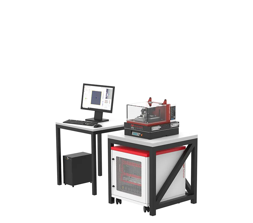
NanoFrazor Scholar
- Thermal Scanning Probe Lithography System
Table-top thermal scanning probe lithography system with in-situ AFM imaging. Compact and compatible with glovebox.